3D imaging solutions are helping semiconductor chip manufacturers meet the industry’s unparalleled requirement for precision, accuracy and scale, finds Jessica Rowbury
Despite the recent chip shortage, and the subsequent glut as companies rushed to build inventories during an economic downturn, chip sales hit a record high in 2022.
According to data from World Semiconductor Trade Statistics, the sale of chips rose globally by 3.2% to $573.5 billion in 2022, following on from the half a billion mark being passed for the first time in 2021.
As OEMs look to further increase the speed, power and intelligence of their products, and as chip manufacturers not only move to larger wafer sizes but also push for fab expansions with help from government incentive schemes, the demand for chips shows no sign of slowing down.
In addition, semiconductor chips are not just growing in volume, but also in complexity, with hundreds of steps involved in their fabrication. Even the slightest deviation from the precise temperature, pressure, and light exposure required for these processes could result in the end product the chip is integrated in not performing as it should. A plethora of inspection tools are therefore used at every stage of the fabrication process, and 3D vision is one such key technology helping chip manufacturers meet the semiconductor industry’s stringent demands for speed, quality and efficiency.
Types of 3D imaging used in semicon inspection
3D imaging tasks in semiconductor inspection range from measuring nanometre-sized defects on wafer substrates to inspecting the overall finished circuit board or end products.
“It's a very wide range of use cases and applications, primarily led by the Asian industry," said Nathaniel Hofmann, product manager for machine vision at Sick UK. “But recent pressures on the supply chain have highlighted the need for fabrication of components around the world. And there will be a number of new fabrication plants starting to crop up in Europe, America and the UK. So we see this is a massively growing market, with a continued push to the advanced [inspection] technologies.”
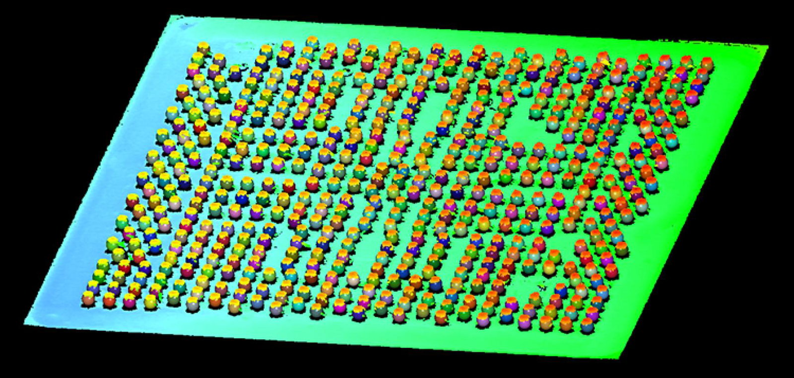
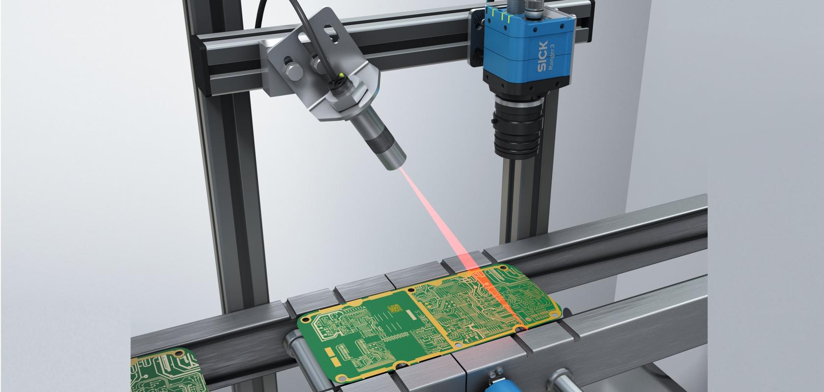
Sick’s 3D imaging products for semiconductor inspection include the Ranger3 series, which employs laser triangulation to test both the functionality and mechanical integrity of the chips during their final inspection as well as as well as the quality of the contact points and their coplanarity in ball grid arrays (BGAs).
Laser triangulation is used to inspect objects moving along a Y axis, whereby a laser line is projected onto the object perpendicular to this axis. The distorted laser profile formed as a result of the varying heights along the object is imaged in a 2D pixel array for each scan. Each image represents a 3D slice in the Y direction of the object, and the row within every column (X) represents the height (Z) of the object at that point.
“It is like slices of bread. A loaf of bread has an overall shape, but it's made up of individual slices. Because you are able to have a very high resolution image profile, and the laser line is very finite in terms of its thickness, you are able to obtain a highly accurate and highly repeatable image,” Hofmann explained.
Different inspection tasks have different requirements, and in the final inspection of chips where tens of thousands of devices are inspected per second, speed is one of the most important factors.
“If Z height location is important, laser triangulation is the most widely accepted with the highest accuracy available to match the production speeds,” said Hofmann. The Ranger3 system can generate up to 46,000 3D profiles per second at an accuracy of five micrometres in the XY direction and 0.5 micrometres in the Z direction.
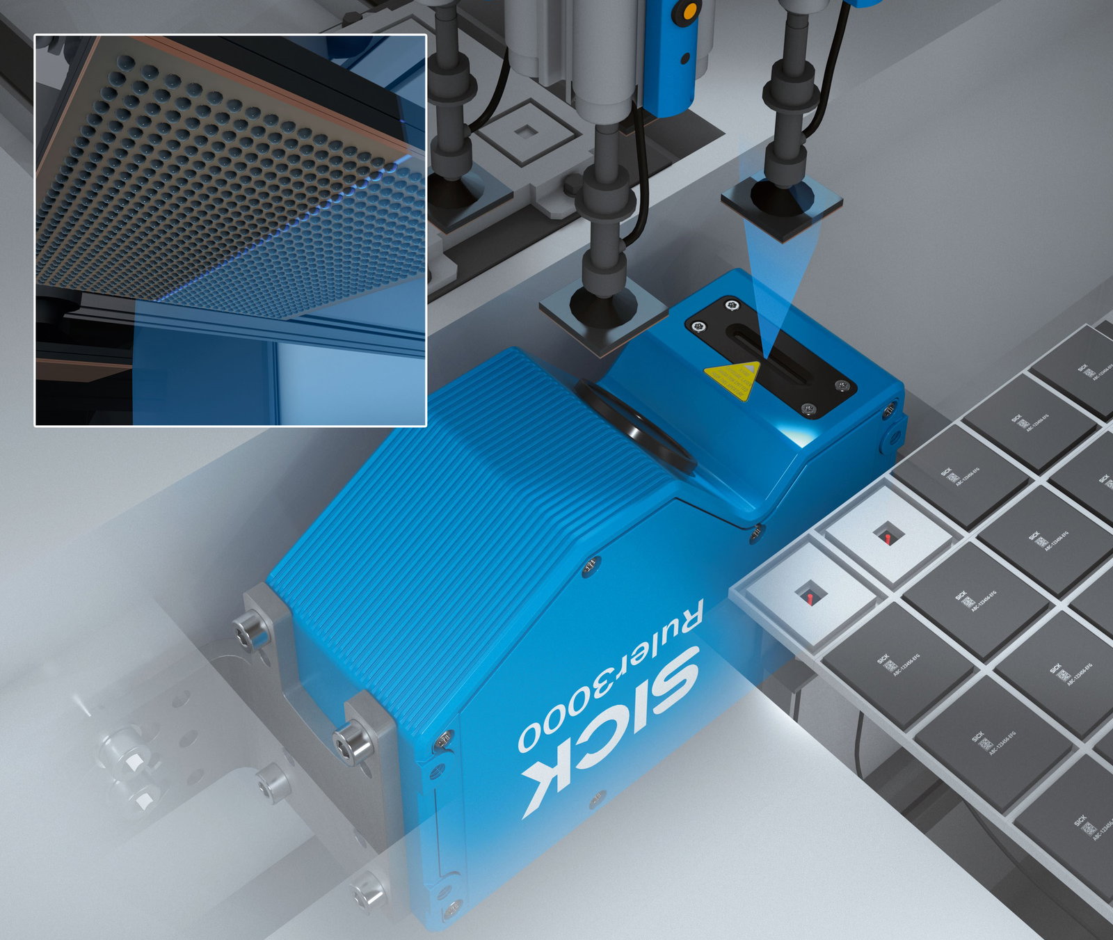
Sick's Ruler3000 camera being used to measure the height and size of solder points on ball grid arrays (Image: Sick)
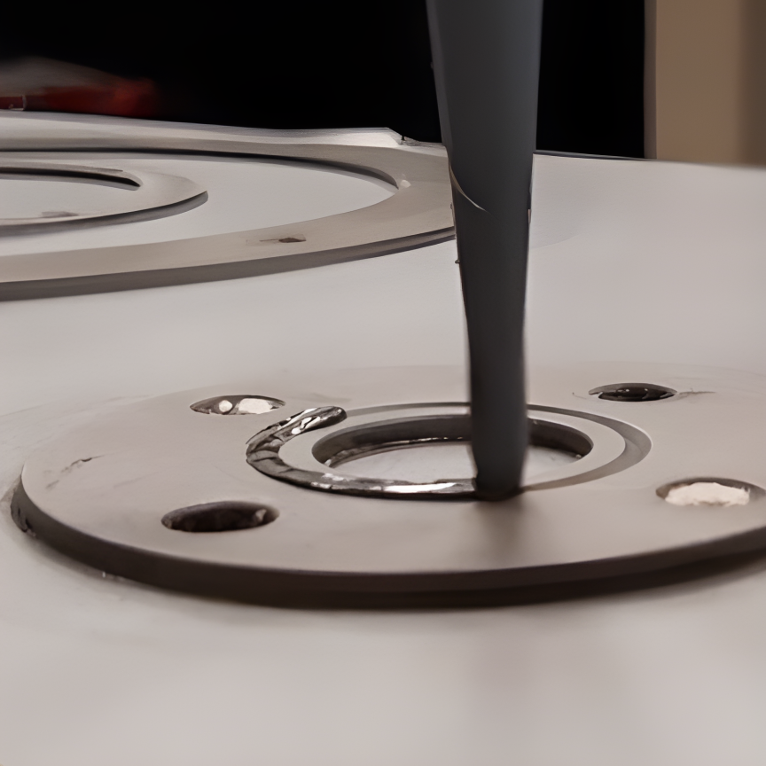
3D line confocal imaging is another technique deployed in semiconductor inspection at the wafer level. LMI Technologies, for example, with its Gocator 5500 series sensors, can measure microscopic-scale dimensions and tomographic structures during wafer inspection. The technique works by projecting a thin line of light onto a target surface and capturing the reflected light with a line-shaped confocal aperture. The confocal aperture filters out any out-of-focus light and only allows the in-focus light to reach the sensor. By scanning the line of light across the target, the sensor’s built-in software can create a 3D point cloud of the scanned surface.
The technique can be used to measure the thickness, flatness, bow, warp, and notch alignment of silicon wafers so they can be sorted. Or, the sensors can scan the surface profile and texture of wafer polishing pads with nanometer resolution to monitor wear or to detect scratches, cracks, or foreign particles.
The technology can also be used to measure end products, such as smartphone screens. In this task, the Gocator 5500 generates three different types of data simultaneously, explained Evan Pontes, Engineering Technologist at LMI Technologies: “When we shoot the light out at an angle we're able to spray the rainbow of different coloured wavelengths across the surface. We’re then able to return it to an imager and read out very accurate data for what's in focus at that particular plane,” he said. “So, as you sweep back and forth over the focal plane of the object, different colours are going to become in or out of focus – and that reaches back to our imager to not only measure really fine resolution, but with particular surfaces like glass or reflective surfaces read multiple layers of the material at the same time.”
In earlier stages of semiconductor manufacturing, sensitivity plays a more important role, as this is where detecting nanometre-sized cracks or contaminant particles on the wafers is the focus. Short-wave infrared (SWIR) imaging is being increasingly used to detect these types of defects on silicon, which has high transmissivity in the SWIR wavelength range. The article covers some of the latest SWIR technologies being deployed for such inspection tasks.
Advances in electronics and imaging go hand in hand
As semiconductor technology advances, so does the technology used to inspect it, Hofmann highlighted: “As the electronics industry continues to push what's possible with the components they are making, this is intrinsically linked to the continued development of both the machine vision hardware and the image processing technology,” he said. “As the processes and the electronics get faster with higher resolutions and processing capabilities, this ultimately benefits the next generation of cameras to provide higher resolution, faster sensors, and faster data output. And by having the faster information coming out of the camera, we can then utilise the improved electronics within computers, GPUs, and so on, to increase the performance of the image processing algorithms, thus speeding up the whole inspection process to offer greater accuracy, greater speed of throughput, or greater resolution.
“As that technology develops, it will also help drive down the cost of lasers, for example, or improve the performance of the optics. So there is a continual push being driven by the electronics industry for development,” Hofmann noted.
But as imaging and machine vision companies might once have focused mainly on R&D and product development, they now must continuously engage with semiconductor OEMs to ensure they stay on top of fast-changing requirements, and to make sure OEMs are educated on how the inspection equipment is evolving.
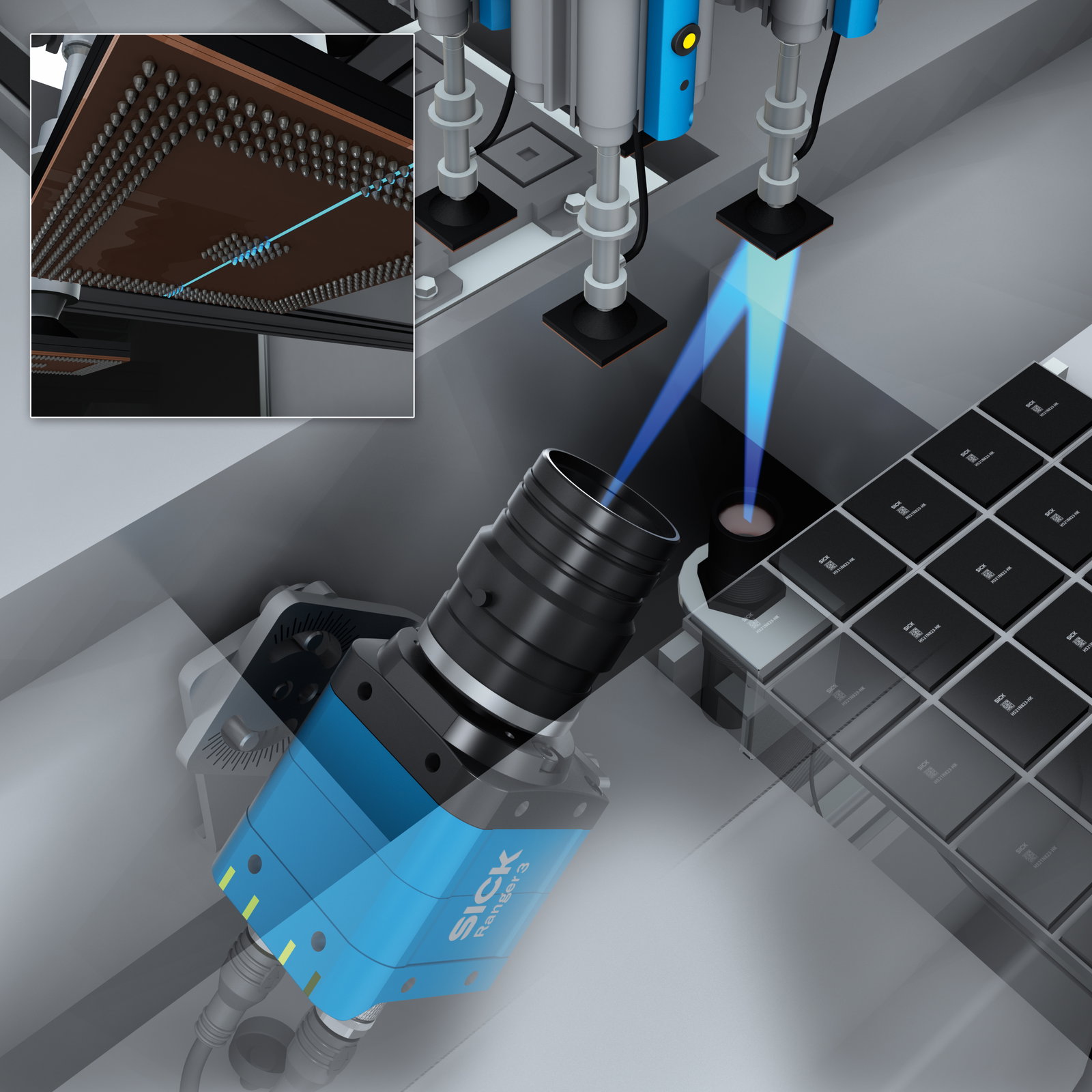
Sick's Ranger3 camera performing 3D inspection and surveying of semiconductor chip connections (Image: Sick)
This is very much the experience of Andreas Hoffman, Director of Technical Services at LMI Technologies, in his 14 years with the company: “When I started, the company was made up of 30-40 people, now it is around 400. We didn’t have tech support for customers back then, there was no application engineering. Everything was done by R&D, and then we created a tech support group which started off being just one person – me. A big part of tech support really is education. We keep adding technology, so the education never stops. We offer training, we go on site and really work with the customer to help integrate, interface or configure the product.”
When it comes to deployment of its Ranger and Ruler series of 3D cameras, Sick’s level of integration involvement depends on customer requirements. Some integrate their solutions in-house or use a third party – particularly if they are incorporating conveyor belt systems, for example. Or, Sick will take a more hands-on approach and work with the customer to optimise the integration of the technology, particularly for customers in Asia, America and Germany.
The biggest integration challenge, according to Sick’s Hofmann, is the customisation of the software needed to make use of the data, because every machine application varies. “Even if you have two production lines side by side, there is a chance there will be differences between the two, which means that from the image processing and the setup side of things, each one potentially has to be treated differently,” he explained. “And when you're at the cutting edge of speed, 3D image processing – which is more complex to start with – accuracy, and absolute repeatability, it's that variability of the inspection task that makes each element a lot more challenging. That combination is why integration is very specialist in the electronics marketplace. You're pushing the boundaries of technology.”
While the semiconductor sector requires numerous inspection modalities, 3D imaging no doubt forms a key part of the industry overcoming its unique challenges of providing accuracy at unprecedented scale.
Read our latest case study: Learn how to install a sensor, scan an object, visualise and evaluate measurement data in less than 10 minutes with new 3D software from AT