Integrated circuits based on semiconductor platforms underpin much of our current technology: everything from electronic devices and sensors to solar panels.
The demand for such platforms is ever increasing, with consultancy firm McKinsey anticipating that the semiconductor industry will be worth more than $1tn by 20301, up from about $600bn in 2021.
It is estimated that about 70% of this growth will be driven by applications in electric vehicles, data storage, and wireless communications.
The need for high-yield, reliable manufacturing processes has pushed the need for excellent semiconductor wafer inspection technologies. Wafer inspection involves imaging semiconductor chips throughout the fabrication process to spot defects.
But the inspection process is costly and time-consuming, with hundreds of steps involved in manufacturing a single chip – a process that can take up to two months. The growing need to address such issues has led to the semiconductor inspection industry itself becoming significant – currently valued at $5bn, and expected to grow to $8.9bn by 2031, according to Allied Market Research2.
Manufacturers continually seek faster, higher-resolution imaging solutions for chip inspection to help boost the rate of fabrication. State-of-the-art cameras are therefore being developed and blue skies research undertaken in a bid to increase yield and efficiency in one of the world’s most important industries.
Short-wave infrared machine vision
Most semiconductor devices are made from silicon wafers. Silicon is largely opaque to visible light, but its transmissivity to light in the short-wave infrared (SWIR) spectrum is much higher, rendering it transparent at wavelengths greater than 1,050nm. As a result, many camera technologies used for chip inspection are based on SWIR sensors. Most of these systems utilise indium gallium arsenide (InGaAs) sensors with a sensitivity range from 900 to 1,700nm. By illuminating silicon semiconductor chips with SWIR light, these cameras can detect tiny features such as micro-cracks or contaminant particles.
“To see small features and failures you need a good signal-to-noise ratio. In order for that, you need a camera that is highly sensitive,” says Marc Larive, Strategic Marketing Manager of Xenics, a sensor and camera developer for semiconductor wafer inspection in chip fabrication.
Xenics’ cameras aim to achieve the vital trade-off between the high sensitivity required for SWIR detectors in semiconductor inspection, and pixel resolution. While the sensitivity of a camera is directly proportional to pixel size, going to smaller pixel sizes is not always the
best solution.
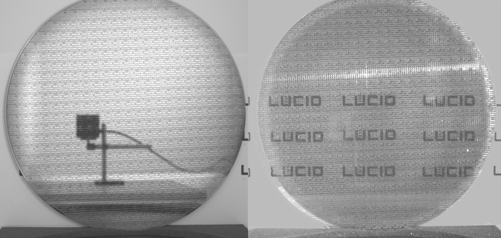
![]()
Lucid Vision Lab’s Atlas and Triton SWIR cameras
“In visible cameras, the aim is to get the smallest pixel size possible, because you can obtain high resolutions,” says Larive. “But in SWIR this isn’t so because you don’t have a lot of natural light. You’re looking for tiny defects, so light budget is an issue. At Xenics, we found a very good trade-off with a pixel size of 20 microns – you can detect very small items, small failures with it.”
The SWIR cameras offered by Xenics are its Wildcat+ 640 series, which use in-house-made InGaAs photodiode detector arrays, 20-micron pixel diameters, and offer speeds of up to 300Hz full frame. Larive says the Wildcat+ 640 offers the highest “normalised sensitivity” (a measure of pixel surface compared with detector noise) available on the market, with high dynamic range. It also comes with a standard industrial interface and triggering abilities – functions that are invaluable to manufacturing clients. Xenics claims to get a normalised sensitivity about 20% higher than most market competitors that use smaller pixel sizes.
While resolution and speed are important metrics, Xenics emphasises that easy integration and compatibility with existing manufacturing infrastructure are also very important. “It’s not rocket science,” says Larive. “But it’s very important for manufacturers so they don’t have to spend years redeveloping technology. It should be something plug-and-play.”
Xenics adds that its products do not just cover SWIR. It also targets long-wave infrared (LWIR) through its Dione CAM product series. LWIR cameras are also of great interest to semiconductor wafer manufacturers, in particular because of their ability to look for thermal defects. The Dione series uses commercially available microbolometers for its sensors.
Lucid Vision Labs is another company making big strides in camera technology for semiconductor inspection. Lucid’s Triton and Atlas ranges both offer SWIR cameras that use Sony 0.3 megapixel IMX 991 and 1.3 megapixel IMX 990 InGaAs sensors. Triton SWIR was launched by Lucid at the beginning of 2023, affording customers a lower-cost alternative to its powerful Atlas series. The Atlas SWIR camera, unlike the Triton range, offers in-camera cooling for decreasing thermal noise in SWIR detection.
Lucid offers a wide range of products for wafer inspection, up to 10 Gigabit Ethernet (10GigE) at resolutions of up to 47 megapixels. Its Atlas model cameras, with up to 31 megapixel resolution, are widely sold, delivering over 5GigE. Lucid is working on pushing the resolution of its cameras even further, aiming to release a 65 megapixel version of the Atlas (Atlas10) camera in Q2 2023. This camera will be Lucid’s highest-resolution model, featuring Gpixel’s GMAX3265 CMOS sensor.
Like other competitors in the industry, Lucid says SWIR cameras are in high demand for semiconductor inspection, but it also produces UV cameras that are used in other parts of the chip-manufacturing process. In December 2022, Lucid launched a UV model of its Atlas10 GigE camera with an 8.1 megapixel Sony IMX487 sensor, capable of imaging between 200 and 400nm.
The bandwidth barrier
While both sensor and camera development are important to Lucid’s technology, the company states that aside from increases in imaging resolution or frame rates, managing bandwidth and data transfer are becoming important areas of growth. In device inspection, for the most efficient defect detection, cameras need high frame rates and high imaging resolution. This creates a huge amount of data. The challenge is then getting this data into a processing computer or GPU, requiring a high bandwidth interface.
“The big question is ‘how should you process all this incoming data?’, ” says Alexis Teissie, Senior Product Manager of Lucid Vision Labs. “On the interfacing side, we are looking at a global view of not just pushing everything to the central CPU, but trying to work closely with our customers to scale with the technology.”
Teissie says it is about leveraging the network standard used in high-performance computing clusters, but applying it to machine vision. “And making sure that we can reliably transfer 10Gigabits from multiple cameras with no CPU involvement,” he continues. “Because we are working with high-frame-rate cameras and we need the highest reliability – and so, high bandwidth – we’re developing special network transfer technology: a Remote DMA technology.”
Remote DMA (RDMA) is a technology that allows networked computers to exchange information without relying on the operating systems or processors of the computers themselves. This technology allows for low latency in the data transfer process, meaning that data packets do not take long to be stored or retrieved. Using RDMA, then, data can be transferred quickly without any burden to the CPU of the processors involved.
“This is a building block to make sure we have reliable transfer so that we can ensure that whenever a frame is required, it will be delivered with certainty,” says Teissie.
“There is this move to go to higher speeds and just getting higher bandwidths – this is just the first step,” Teissie adds. “25GigE
is coming.”
Lucid’s upcoming Atlas10 camera with RDMA is aimed to be released by the end of Q2 2023, and it notes that “one of the target markets for this is definitely semiconductor wafer inspection”.
Quantum vision
One limiting factor surrounding SWIR cameras based on InGaAs sensors is their price point, which can stretch to thousands of euros per sensor chip because of their fabrication process. SWIR sensors utilising quantum dots (QDs) have, in the past few years, provided a potential route to lowering costs. These sensors, which are based on thin films, use QDs as a detection mechanism for SWIR radiation.
QDs are now disrupting the marketplace for SWIR cameras, being deployed in products such as SWIR Vision Systems’ Acuros series and Emberion’s VS20 Vis-SWIR camera. The Acuros cameras use a 15 micron pixel size in their detectors, as well as offering camera cooling technology to reduce the impact of thermal noise. Emberion is also developing a version of its VS20 series with a GigE interface, potentially offering a framerate of up to 400fps.
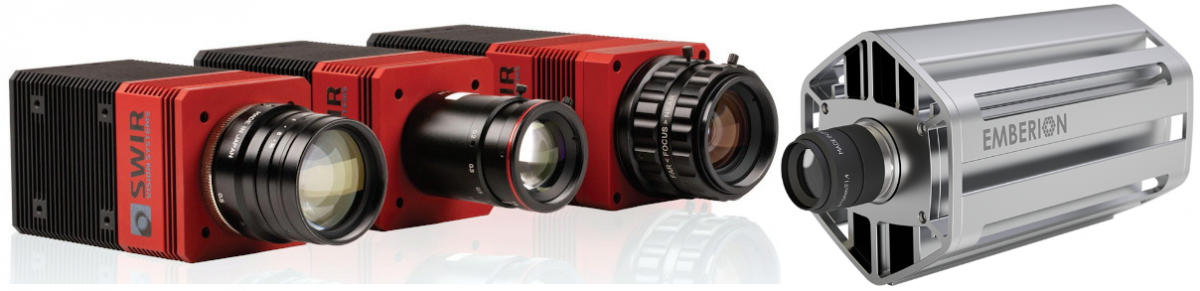
SWIR Vision Systems’ Acuros camera, left, and Emberion’s VS20 Vis-SWIR, right, are both based on sensors utilising quantum dot technology
“QD-based SWIR cameras are already on the market, costing around half the price of conventional alternatives,” says Dr Hao Pang, CEO and Founder of Quantum Science, a specialist nanomaterials developer that uses a new fabrication technique to push down the price of QD-based SWIR sensors even further. Its in-house-developed INFIQ QDs are produced at scale using a synthetic process that facilitates control and production. This enables them, in Pang’s words, to manufacture SWIR sensors “at a fraction of the price of existing technologies”.
“Traditional formation processes involve the deposition of 14-16 thin film layers, which introduce multiple opportunities for manufacturing errors to occur. INFIQ QDs can be deposited in a single layer. This minimises the risk of defects forming and accelerates the manufacturing process.”
Quantum Science’s QD fabrication also circumvents another barrier to the wide adoption of QDs: the toxicity of heavy metal components used in their manufacture. The company is already partnering with sensor design companies and large semiconductor businesses with the aim of bringing its QDs to market quickly.
Blue skies ahead
Promising advances for potential applications in semiconductor inspection are also happening in academia. Jinyang Liang’s team at INRS at the Université du Québec, Canada, has recently released a new camera based on single-pixel imaging technology, described in Nature Communications3.
Single-pixel imaging is a computational imaging technology that relies not only on the optical image collected by a detector, but the use of a computer to reconstruct the image: technology that brings together both optical engineering and computer science.
“The marriage of these two fields can give you many unique aspects that allow imaging systems to exceed the technical capabilities of conventional imaging systems,” says Liang. “The focus of our research is towards the high-speed [imaging] aspect.”
Liang’s research is describing cameras that operate with frame rates of up to one million frames a second. At the moment, the technology exists only in the visible, but Liang and his team are looking at commercialising their cameras for applications to long-wave infrared and terahertz imaging – potentially of interest to semiconductor wafer inspection.
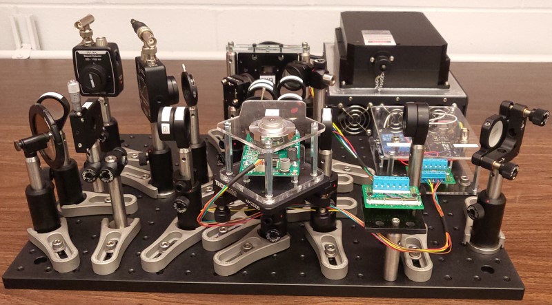
Liang et al.’s setup for combining single-pixel and terahertz imaging techniques, which could offer an excellent solution for non-invasive semiconductor inspection
“Combining this [single-pixel imaging] technique with terahertz imaging could be a very nice potential technique for non-invasive semiconductor inspection because it’s sensitive to the flow of charges,” he says. “We may be able to see the flow of charges to see where there might be a broken wire or malfunctioning chip.”
This kind of inspection is currently done by first capturing an image and then extracting positional information on a shot-by-shot basis, which is time-consuming. However, Liang sees single-pixel imaging as a technique for potentially dramatically increasing inspection speed. “The advantage would be that you have much faster image rates,” he said.
Liang’s research is still in its development phase, though the team has partnered with Agile Light Industries to work on applying their research to existing commercial sensors.
“For the technique we’ve developed, the technological readiness level is rather high,” says Liang. “Right now, we are working on jointly developing this technology further, to turn it into a compact and turnkey device.”
The wafer inspection industry is one where research such as Liang’s is filtering quickly into commercial products, mirroring a dynamic and uncompromising manufacturing environment. With others such as Lucid, Xenics and Quantum Science bringing new, blue-skies innovation into their own product lines, the future of chip inspection certainly looks bright.
Lead image: Lucid Vision Labs
References
- McKinsey & Company – ‘The semiconductor decade: A trillion-dollar industry’
- Allied Market Research – ‘Semiconductor Inspection System Market Research, 2031’
- Kilcullen, P., Ozaki, T. & Liang, J. ‘Compressed ultrahigh-speed single-pixel imaging by swept aggregate patterns’, Nature Communications 13, 7879 (2022).
Sponsored: Meeting the demands of high-throughput semiconductor inspection
Maximilian Klammer and Klaus Riemer share how colour line scan CMOS cameras are enabling high-throughput inspection for semiconductor and PCB manufacturing
Semiconductor geometries and printed circuit board (PCB) components are becoming smaller, while the demands on quality testing and control are growing.
Because of the minute structures involved, optical inspection in modern semiconductor manufacturing occurs in the micrometre range. The need to detect defects and contamination at this scale and at high throughput places the highest demands on inspection systems. Extremely high-resolution colour line scan cameras with CMOS technology have been developed to accomplish this.
CMOS technology
Line scan cameras are suitable for image-capturing tasks where fast-moving large areas or flat objects must be captured and analysed with high optical resolution. In a CCD line scan camera, the pixels of the sensor are arranged in a single line. The readout cycle is adapted to the throughput speed of the inspected objects or surface areas. The whole two-dimensional image is then created by joining the individual lines together.
CCD sensors have long been the technology of choice in line scan imaging because of their image quality, high sensitivity, low noise, low photo-response non-uniformity (PRNU), high dynamic range, and signal-to-noise ratio. These benefits are essential in line scanning because of the high-speed image acquisition and reduced number of photosensitive cells, which means exposure is limited.
New-generation CMOS line scan sensors now offer similar image quality to CCDs, coupled with benefits such as higher readout speed and flexible readout modes. Unlike single-line CCDs, these sensors have several lines of pixels, allowing for different operation modes depending on an application’s requirements. One key benefit of a multiline sensor is time delay integration (TDI). TDI consists of adding up the values of adjacent pixel lines synchronously with the motion of the object below the camera. The same section of the object is imaged by several lines, and adding up the signals of all these lines increases the signal intensity compared with a single line sensor. This solution has a much better signal-to-noise ratio than an equal increase in gain.
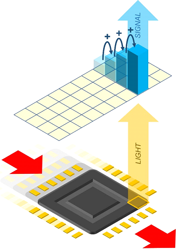
With time delay integration, the same point on the object is captured by all pixels of the same column as the object passes below the sensor. The signals of all pixels are added up to increase sensitivity
The combination of specially adapted line illumination with CMOS line scan cameras results in a powerful system optimally matched to the application. The illumination system homogeneously illuminates a line on the object with a very high luminosity, whereby the light colour and the illumination geometry can be precisely adapted to the image capture requirements.
Profitability in semiconductor manufacturing relies on the level of flawless product yield. Therefore, manufacturers test products multiple times, starting with bare wafers and ending with inserting the chips into the IC packages.
As the wafer moves along the production line, components are added, increasing its complexity. Yield-reducing defects must therefore be identified as quickly and as early as possible while also reducing overall inspection time. This results in more inspection points at each process step in the production line, with the inspection system required to produce the scan results more quickly. Inspection throughput is critical to the fab’s overall production.
Faster semiconductor inspection
Scanning and illumination techniques offer a solution by providing faster and more efficient semiconductor inspection. As a rule, wafer inspection is performed with dark-field illumination and coaxial bright-field illumination. PCBs can be inspected using a combination of diffuse light and bright-field illumination – the diffuse light is used primarily for 3D-shaped components to eliminate gloss and reflections while the bright-field lighting is used to inspect the substrate itself.
New-generation cameras feature multichannel illumination functionalities that enable different types of illumination in one scan. Acquiring up to four different images in one scan provides much more information and improves defect detection. Multifield imaging enables the generation of HDR images from up to four lines captured with different settings. This allows details to be detected in both bright and dark areas in the image. Both can be combined to increase detection reliability and shorten inspection time.
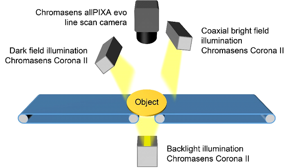
Chromasens’ allPIXA evo allows up to four lighting configurations to be combined in one scan. Three different light configurations are shown here
The trend toward miniaturisation continues for PCBs and the components mounted on them. This leads to so-called panelisation, whereby several PCBs are manufactured on one panel. Each PCB on the panel is identified by a unique barcode, and thus rapidly inspecting the PCBs is correspondingly complex and demanding. For example, during the visual inspection, existing solder defects, such as interruptions, solder bridges, solder short circuits, or excess solder, must be identified, in addition to component defects such as lifted solder and missing or misplaced components. A colour line scan camera system can perform these inspection tasks with great accuracy because of its high operating speed and lateral resolution. Oxidised copper wires on PCBs must also be detected, yet monochrome systems cannot reliably identify oxidised areas. However, high-performance colour line scan cameras such as the allPIXA evo from Chromasens, combined with high-performance illumination, excel at this task.
Examples from semiconductor and PCB manufacturing show that high-performance colour line scan cameras can play an important role as central components in 100% real-time inspection processes. The image quality and resolution performance of multiline full-colour CMOS line sensors result in a particularly high application potential for camera systems. Fast and accurate colour measurements and rapid 3D inspection are additional future applications.
Maximilian Klammer is an R&D Manager and Klaus Riemer a Project Manager at Chromasens GmbH.