Skip to main content
Social media links IMVE
LinkedIn
Twitter
Log in
Register
Applications
3D
AI/ Deep learning
Embedded
Hyperspectral
Robotics
Thermal & Infrared
Components
Cabling
Cameras
Illumination
Image processing
Optics
Sensors
Software
Industries
Agriculture & Food
Life Sciences
Logistics
Manufacturing
Security & Defence
Sports & Entertainment
Traffic & Transport
Visionaries
Resources
Buyers' Guide / Suppliers
Events
Products
Webcasts
White papers
Search
“It’s not a magic box”: Building a vision system with scale
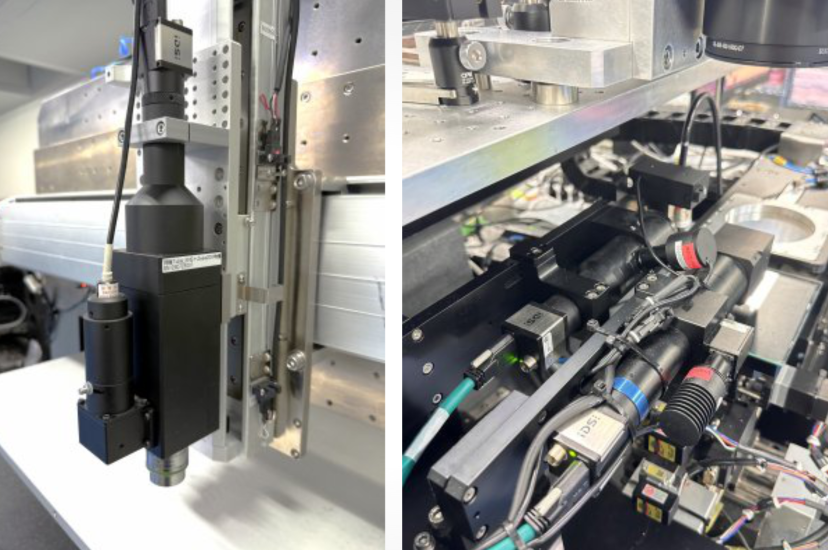
Micraft System Plus integrates cameras for micro-LED transfer and die stacking
36ZERO Vision’s AI inspection platform secures €3.6m to scale with industrial imaging
Join our expert roundtable on 3D vision technology's transformative impact
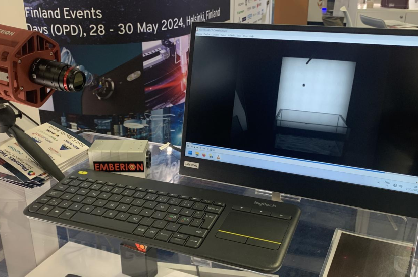
Emberion showcases high-speed, compact SWIR imaging solutions at Photonics West 2024
Omron's SWIR camera overcomes manufacturing challenges
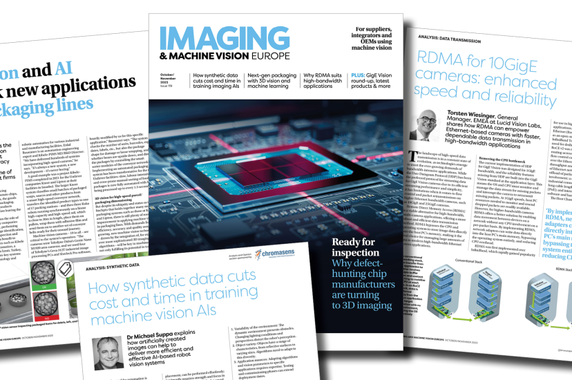
The latest issue of Imaging & Machine Vision Europe is out now!
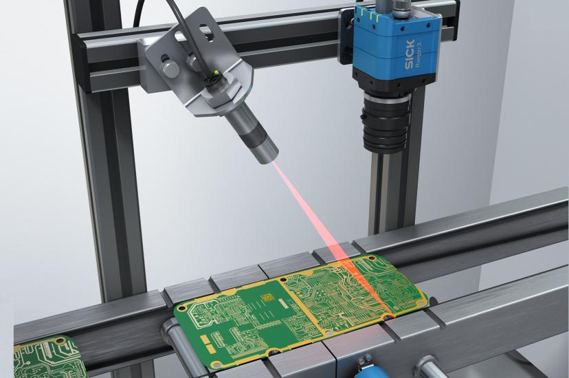
3D vision helps address semiconductor inspection challenges
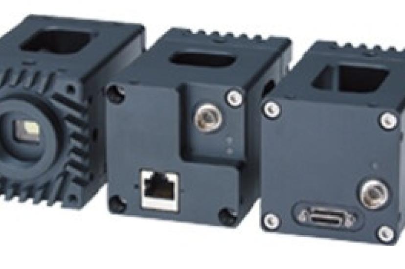
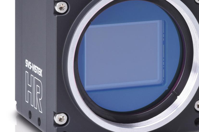
SVS-Vistek launches camera for semiconductor inspection
The latest development trends of the machine vision market
Pagination
Page 1
Next page
››
Media Partners