Technology that advances 3D imaging, makes lenses more resistant to vibration, turns a CMOS camera virtually into a CCD, and makes SWIR imaging less expensive, are all innovations that have been shortlisted for this year’s Vision Award, to be presented at the Vision show in Stuttgart, Germany.
Other shortlisted entries include a new system-on-chip for vision and a sensor that does away with recording images frame-by-frame. The winner will be announced during the Vision trade fair, when it takes place in Stuttgart from 6 to 8 November.
An independent jury of machine vision experts selected the seven shortlisted entrants, which includes technology from The Austrian Institute of Technology, Basler, the Fraunhofer Institute for Integrated Circuits, Fujifilm, Photoneo, Prophesee, and SWIR Vision Systems.
Imaging and Machine Vision Europe is proud to sponsor the award, which highlights outstanding innovations in machine vision.
Japanese lighting company, Machine Vision Lighting, won the 2016 Vision Award for its VISA-Method Lighting, which is able to give uniform illuminance of light irrespective of distance from an object.
Here, we take a detailed look at the technology behind the seven shortlisted entries.
Inline Computational Imaging: Single sensor technology for simultaneous 2D and 3D high definition inline inspection
By Svorad Stolc, Petra Thanner, and Markus Clabian, Austrian Institute of Technology
The Austrian Institute of Technology's (AIT) Inline Computational Imaging (ICI) platform is an industrial inline inspection system based on a single camera, which is capable of simultaneous colour 2D and 3D inspection. The solution combines light field and photometric stereo imaging techniques, and is developed for high-performance industrial inline inspection.
Light field and photometric stereo are computational imaging methods using several images of an object to reconstruct it in 3D. The light field technique takes multiple images from different observation angles to give good absolute depth accuracy, while photometric stereo makes use of different illumination angles to image fine surface details. The AIT ICI system combines the advantages of both techniques, together with line scan imaging.
A matrix camera fitted with a standard non-telecentric lens and two static light sources is used in a multi-line scan mode, with only a small number of line-pairs read out while the object moves underneath the camera. Each of these line-pairs acts as an individual line scan camera, producing an image stack containing light field information stemming from different viewing angles, and photometric information stemming from different illumination angles.
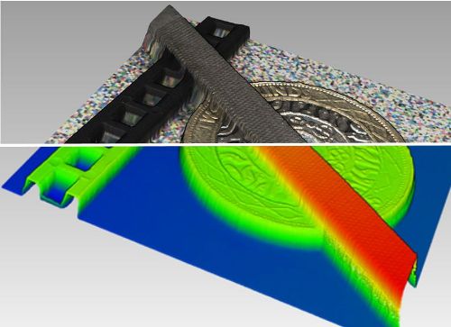
The ICI 3D reconstruction algorithms are a combination of depth analysis and surface reconstruction. For the light field depth analysis, the acquisitions are represented as an epipolar plane image (EPI) stack. The slopes (angles) of the EPI linear structures correspond to the depths of each image position. Depth analysis is performed using a multi-view correspondence analysis in the EPI domain with tailored image features that are insensitive to brightness and contrast variations.
In the photometric stereo analysis, surface orientations are derived from local shading information. Although, the surface geometry can be partly retrieved from surface orientations only, the ICI method combines the depth estimation from the light field and photometric stereo analyses to achieve improved reconstruction accuracy. Final 3D reconstruction is delivered as a point cloud together with measurement confidence values for each single captured point. Besides the 3D point cloud, pixel-rectified colour images are also captured.
AIT ICI comes with a tailored bundle adjustment algorithm for inline compensation of motion artefacts. This makes the solution very robust and allows for high magnification down to 4μm per pixel lateral resolution.
Typically, the system runs at 20kHz at 11 lines. Multi-line scan rates up to 150kHz are feasible using four lines and a high-speed camera by AIT. This makes ICI suitable for a broad range of industrial inspection tasks. All algorithms are fast and accurate enough for high-performance inline inspection. All outputs are provided in standard image formats so they can be processed using standard machine vision libraries.
The AIT ICI technology aims to close the gap between 3D machine vision systems offering either high optical resolutions or high inspection speeds. The AIT ICI is a rather simple yet powerful acquisition concept. In combination with smart algorithms it enables a new dimension in fast and accurate inline inspection.
https://www.ait.ac.at/en/research-fields/high-performance-vision/inline…
EMVA1288 compliant interpolation algorithm
By Jörg Kunze, Basler
Basler has invented an interpolation algorithm, called the Virtual Pixel Interpolation, which creates values of virtual pixels at given positions and with a common given size, thereby fulfilling all EMVA 1288 requirements for real pixels. This allows an easy replacement of old CCD cameras with new CMOS cameras without changing the optical setup or software of the application.
The availability of many CCD image sensors is limited in time and volume. The latest CMOS image sensors offer high pixel count and great image quality, but they are often not one-to-one replacements for CCDs, because the pixels are generally smaller. This means replacing a CCD camera with a CMOS model could require costly changes in application optics and software.
Basler’s Virtual Pixel Interpolation serves as a technological base for a one-to-one replacement of a CCD camera by a CMOS camera sensor. It creates images consisting of virtual pixels of the same size as the replaced CCD image sensor, complying with EMVA 1288.
To emulate a CCD sensor image with 5.6μm pixels using an image taken by a new CMOS sensor with smaller pixels of 3.6μm, for example, basically requires creating an image with lower resolution.
Sub-sampling and binning lower the image sensor resolution, but both methods only work for integer factors in horizontal and vertical resolution. This isn’t normally the case for the ratio between CCD and CMOS pixel sizes. Interpolation is a well-known technique to change the resolution of camera images; nearest-neighbour, (bi-) linear, and (bi-) cubic interpolation are often used. However, interpolated images frequently raise concerns in the machine vision community, because state-of-the-art interpolations can create pixels of different sizes and gain factors.
After one year of research, Basler identified an efficient computable solution. The Virtual Pixel Interpolation algorithm runs well even on a small 8-bit controller and enables real-time application. This is mandatory for machine vision applications.
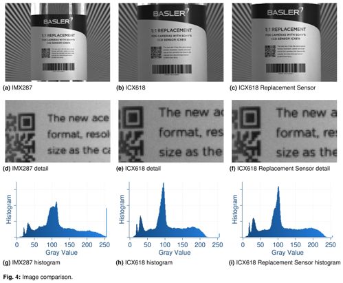
The new camera image in Fig. 4c matches the ICX618 image in Fig. 4b well, whereas the IMX287 image in Fig. 4a clearly differs in field of view. The same findings hold true when zooming into the details. Also, the histogram of IMX287 in Fig. 4g is clearly different from the original ICX618 histogram in Fig. 4h, whereas the ICX618 Replacement Sensor shows a perfect match in Fig. 4i.
A two-dimensional Virtual Pixel Interpolation has been tested on the ICX618 CCD raw image series for different resolutions. An EMVA 1288 report has been created for each resolution. All of the EMVA 1288 reports contained plausible results that were exactly as expected for a CCD image sensor with the respective pixel size. All QE values are exactly as expected within a small error bar and equal the original ICX618 QE value for the used wavelength.
The Basler AcA640-121gm is the first CCD replacement camera incorporating this technology. Further 1:1 CCD replacement camera models are expected in the near future. The camera has been directly compared to two conventional Basler Ace cameras, one containing an original ICX618 CCD and the other containing an IMX287 CMOS. The latter has been proposed by Sony as successor for the ICX618. All three cameras have been tested in an optical lab using identical lenses and target scenes at different lighting conditions and different wavelengths.
The replacement is cost-efficient and easy; no further changes in application optics, mechanics, or software are expected. This saves cost in development, production and logistics for re-designs of vision machines.
A software-programmable vision system-on-chip for high-speed image acquisition and processing
By Jens Döge, Christoph Hoppe, Peter Reichel, Nico Peter, Ludger Irsig, Christian Skubich, Patrick Russell, and Andreas Reichel, Fraunhofer Institute for Integrated Circuits
The IAP VSoC2M is a novel member of the Fraunhofer vision system-on-chip (VSoC) family for high-performance image acquisition and processing applications. It combines analogue convolution during the readout process; fast column-parallel processing for image analysis and feature extraction, including analogue storage and software-defined analogue-to-digital (A/D) converters; an asynchronous readout path for sparse data compression; and an application-specific instruction set processor (ASIP) concept for software-defined process control.
This enables many new possibilities in embedded image processing, from content-based multi-region of interest (ROI) image acquisition via optical measurement methods such as laser light sheet triangulation or optical coherence tomography (OCT), to feature-based process control.
Applications such as laser light sheet triangulation or OCT rely on a few or small ROIs, and certain optical control tasks may only require scalar output. Thus, reducing the amount of data as early as possible speeds up A/D conversion and subsequent processing steps, mitigating the digital interface bottleneck of traditional high-speed image sensors. A VSoC eliminates the need for external image processing hardware, enables latency below 100μs, and full frame rates above 10kHz.
VSoC2M consists of a two-megapixel charge-based pixel matrix, enabling analogue-digital column-parallel pre-processing via 1,024 processor elements. Each processor element contains 32 analogue memory cells, a dedicated AD/DA converter and basic digital processing functions.
An ASIP controls the VSoC's functional units, including line control. A compacting readout pipeline operating in parallel to data processing means the VSoC can be used for event-based, compressed sensing and conventional methods with continuous data streams. Software is developed in Python with embedded Assembler.
High-speed image sensors with integrated signal processing have been widely used for measurement applications (the Sick IVP Ranger, for example) since the 2000s. Convolutional neural network-based sensors, such as the Teledyne Anafocus Eye-RIS, are not yet as prevalent in industrial imaging due to relatively low image resolution.
The VSoC concept of column-parallel, charge-based signal processing and flexible ASIP-based control enables 1D analogue convolution operations and software-defined digitisation. VSoC2M significantly improves upon its predecessor's readout speed and flexibility with new methods for row- and column-wise data compression.
VSoC2M excels in applications with high frame rate and/or latency demands, and procedures requiring compression of features or scalars. Its flexible, software-defined nature means OEM VSoC modules can be adapted to customers' needs and opens up many new possibilities in embedded image processing, ranging from content-based multi-ROI image acquisition via optical measurement methods (such as laser light sheet triangulation and OCT) to low latency process control.
https://www.eas.iis.fraunhofer.de/en/research_topics/industrial_image_p…
New camera lens design for shock and vibration resistance
By Nina Kürten, Fujifilm Optical Devices Europe
Industrial imaging systems are frequently subject to strong acceleration, shock, and vibration. This is especially true for mobile systems, like robot-guided 3D scanners, but also for fixed installations. Such mechanical stress often causes a significant reduction in the resolution and a shift in the optical axis – a severe problem for machine vision, optical metrology applications, and optically calibrated systems.
Fujifilm investigated the impact of shock and vibration on industrial fixed focal length lenses and from this work developed a new mechanical design for lenses, the Fujinon Anti-Shock and Vibration technology. This technology is based on elastic fixation of the glass elements inside a lens. It minimises adhesives that are used to fix glass elements within conventional camera lenses. Adhesives are unable to withstand shock and vibration over time, causing the glass elements inside lenses to loosen and the resolution and mechanical stability to degrade. The elastic fixation used in Anti-Shock and Vibration lenses gives a constant performance and high image quality over time.
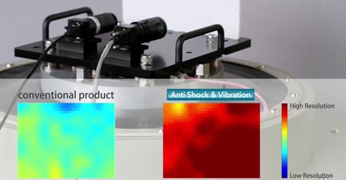
Tests showed a deterioration of the resolving power after vibration with conventional lenses
Fujifilm tested industrial fixed length focal lenses with, firstly, 10G shocks applied from six different directions orthogonal to the optical axis. Next, a special vibrating table exposed the lenses to various sinusoidal vibrations according to IEC 60068-2-6 (up to 500Hz and 100m/s²). Finally, the shock test was repeated.
The tests showed that the position of the optical axis shifted by up to 26μm with conventional lenses. That corresponds to a change of approximately 7 pixels for second generation Sony Pregius sensors with a pixel size of 3.45μm. Such a shift in the optical axis is not acceptable for calibrated systems such as 3D scanners or for metrology applications.
The resolving power of the lenses was checked before and after the test with a ‘text chart’, which gives the resolution of a lens across the entire image simultaneously by measuring the contrast of text. The contrast measurement was transferred via a Fujifilm software tool to a resolution map showing high resolution in red and low resolution in blue. The test showed a deterioration in the resolving power of conventional lenses after vibration. For most machine vision applications, where fast acceleration and strong vibration can occur, these lenses are not suitable.
The shift in optical axis is reduced significantly in Fujinon machine vision lenses incorporating the Anti-Shock and Vibration technology. The lenses withstood shocks showing a shift in optical axis of between 4μm and 10μm. The resolving power also remained stable during and after the vibration test, and the resolution degradation is minimised across the entire image.
Compared to conventional products, these Anti-Shock and Vibration lenses maintain their high optical performance despite the shock and vibration that unavoidably occur in industrial imaging systems.
https://www.fujifilm.eu/eu/products/optical-devices/cctv-and-machine-vi…
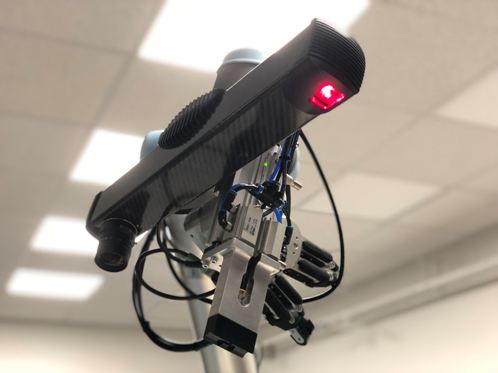
PhoXi 3D camera
By Tomas Kovacovsky and Jan Zizka, Photoneo
Photoneo's PhoXi 3D camera captures accurate point clouds combined with a standard intensity image. It is based on Photoneo's technology called Parallel Structured Light implemented on a custom CMOS image sensor. The novel approach gives efficient, high resolution scanning in motion.
Photoneo's Parallel Structured Light technique projects and captures multiple encoded patterns at the same time. This is done by using pixel modulations inside the company’s custom CMOS sensor. The sensor is divided into several groups of individually modulated pixels, which work synchronously with a laser light projector. Instead of modulating the projection itself, the coded patterns are injected into the groups. At the end of the frame, the sensor can produce more than 20 different virtual images of the scene lit by the coded patterns. The technique can use any kind of sequential structured light pattern, and can adapt to different materials and light situations. The virtual images are then processed onboard the camera.
In the ‘one-frame’ camera mode, the sensor provides 1,068 x 800 resolution output at up to 60fps. These points are interpolated from around 500,000 individual measurements. The typical standard deviation of z-noise at 1m distance is less than 0.5mm. The sensor uses 4.5 pixels per 3D measurement with sub-pixel accuracy coding (high z-accuracy), which gives a high XYZ resolution.
The other mode of operation is a scanner mode designed for static scenes. Here, the sensor returns its raw output of 1,602 x 1,200 individual measurements. This is captured in three subsequent frames. The projection unit lights the scene with a laser deflected by a mirror. The per-pixel exposure of the projection is 10μs, which ensures motion blur-free, consistent data.
All Photoneo's sensors are equipped with a band-pass filter that reduces ambient light. In addition, Photoneo's active ambient light suppression is able to work in sync with the projector and the sensor to control light sensitivity at the sensor surface. At any given time during the acquisition, only about one per cent of the sensor surface can be exposed to direct reflections. The camera's control circuit can disable the rest of the sensor (99 per cent) so that it does not collect any photoelectrons. The technology effectively suppresses the ambient light of any source by a ratio of 1:100 and thus allows scanning under direct sunlight.
The same technology also suppresses internal inter-reflections between pixels by the same ratio of 1:100. When two sensors operate together in the same area, the technique rejects the second scanner’s projection in 99 per cent of the image, and the remaining one per cent of pixels can be filtered out from the result.
The PhoXi 3D camera can capture sub-millimetre details, while its ability to scan rapidly moving objects allows it to be used in almost any situation. Potential applications for the camera include: bin picking; palletising and depalletising; quality control and metrology; autonomous delivery systems; people counting and behaviour monitoring; object sorting; face recognition; and in agriculture.
Event-based vision enables the next revolution in visual perception for machines
By C. Posch and S. Lavizzari, Prophesee
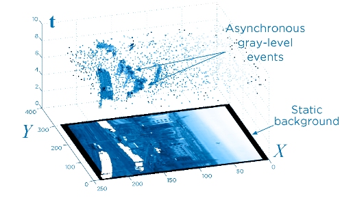
Prophesee has developed an image sensor, the output of which is not a sequence of images but a time-continuous stream of individual pixel data, generated and transmitted conditionally, based on what is happening in the scene.
The sensor contains an array of autonomously operating pixels that combine an asynchronous level-crossing detector with a separate exposure measurement circuit. Inspired by biology, every pixel in the sensor optimises its own sampling depending on the visual information it sees. In the case of rapid changes, the pixel samples at a high rate; if nothing happens, the pixel stops acquiring redundant data and goes idle. Hence each pixel independently samples its illuminance upon detection of a change of a certain magnitude in the light level.
The result of the exposure measurement – i.e. the new grey level – is asynchronously output from the sensor together with the pixel's coordinates in the sensor array. As a result, image information is not acquired and transmitted frame-wise, but continuously, and conditionally only from parts of the scene where there is new visual information. Or, in other words, only information that is relevant – because unknown – is acquired, transmitted, stored and eventually processed by machine vision algorithms.
Pixel acquisition and readout times of milliseconds to microseconds are achieved, resulting in temporal resolutions equivalent to conventional sensors running at tens to hundreds of thousands of frames per second. As the temporal resolution of the image data sampling process is no longer governed by a fixed clock driving all pixels, data volume depends on the dynamic contents of the scene. Visual data acquisition simultaneously becomes fast and sparse, leading to ultra-high-speed acquisition combined with reduced power consumption, transmission bandwidth and memory requirements.
The exposure measurement is asynchronously output from the sensor together with the pixel's coordinates in the sensor array
In addition, processing algorithms now work on continuous time events and features instead of on discrete static images. The mathematics that describe these features in space and time are simple and elegant, and yield highly efficient algorithms and computational rules that allow for real-time operation of sensory processing systems while minimising demand on computing power. And thanks to the time-based encoding of illumination information, very high dynamic range – intra-scene DR of 143dB static and 125dB at 30fps equivalent temporal resolution – is achieved.
Prophesee has launched an advanced event-based reference system called Onboard. It integrates a third generation VGA sensor camera module with MIPI CSI interface, into a powerful reference vision system Arm-based quad-core platform. It provides comprehensive connectivity including Ethernet, USB, HDMI, Wi-Fi, operating under a Linux OS.
The embedded system runs dedicated computer vision software. Currently, it offers a tracking algorithm to detect motion, segment data into groups of spatio-temporal events, and track over time, taking two out of the four available cores. The application layer comprises area monitoring, high-speed counting, vibration measurement and real-time inspection, which makes Onboard the perfect fit for the new artificial vision capabilities demanded by the fourth industrial revolution.
Novel machine vision cameras featuring CQD sensors for high resolution, lower cost SWIR imaging
By George Wildeman and Ethan Klem, SWIR Vision Systems
SWIR Vision Systems is introducing a new class of cameras featuring a 400nm to 1,700nm broadband image sensor technology based on colloidal quantum dot (CQD) thin film photodiodes fabricated monolithically on silicon readout wafers. These sensors have the potential to achieve for SWIR imaging, what CMOS image sensors and micro-bolometer arrays have achieved for visible and longwave infrared imaging respectively. Namely, to leverage the scale and cost structure of the silicon integrated circuit industry, moving SWIR imaging from a specialised niche into broad commercial markets.
The current SWIR imaging market is dominated by indium gallium arsenide (InGaAs) sensors, a compound semiconductor grown epitaxially on lattice-matched indium phosphide (InP) substrates. The fabrication method imposes limitations on pixel size, pixel spacing, and sensor resolution; commercially practical InGaAs SWIR cameras are limited to VGA resolution, and even these are considered too costly for most machine vision applications.
Conversely, SWIR Vision Systems’ CQD sensor technology uses a monolithic integration approach, in which the quantum dot-based sensor is fabricated directly onto CMOS readout integrated circuits (ROICs) using well-established, low-cost semiconductor deposition techniques. The process requires no hybridisation, no epitaxial growth or exotic substrate materials, no pixel-level sensor patterning, and can be easily scaled to wafer-level fabrication. The approach also employs low-cost, solution-processed lead sulphide (PbS) colloidal quantum dots to form as small as 3µm pitch p-n photodiode arrays sensitive in both the SWIR and visible spectral bands.
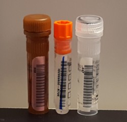
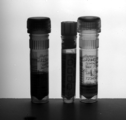
Imaging of fill levels in plastic pharmaceutical vials: colour image (left) and SWIR CQD camera image (right)
The relative crystalline disorder of colloidal quantum dots currently results in lower quantum efficiency when compared to InGaAs cameras, which may make these cameras less suitable for photon-starved applications. However, in the majority of machine vision applications a CQD sensor-based camera can be paired with relatively inexpensive active illumination, resulting in near InGaAs equivalent performance with a significant reduction in overall system cost.
To demonstrate applicability to imaging applications, SWIR Vision Systems has fabricated 2D arrays of quantum dot-based photodiodes on numerous commercial-off-the-shelf silicon CMOS ROICs and integrated them with corresponding camera electronics. The company is releasing the production Acuros camera family featuring: InGaAs equivalent noise, pixel operability greater than 99 per cent, 15µm pixel pitch, and three different pixel array sensor formats (640 x 512, 1,280 x 1,024, and 1,920 x 1,080). The cameras are capable of imaging at speeds up to 380fps via GenICam-compliant GigE Vision and USB3 Vision interfaces.
CQD camera sensors fabricated with low cost materials and CMOS-compatible fabrication techniques represent a major advance towards broadly accessible high definition SWIR imaging. SWIR Vision Systems expects the camera's lower cost points and its non-ITAR, EAR99 export classification to drive higher adoption rates globally, broadening the market for SWIR camera technology.
This technology will open up applications that InGaAs cameras cannot reach today because of constraints on image resolution, or due to their higher intrinsic cost.