To date, the shortwave infrared sector has been dominated by sensors based on indium gallium arsenide (InGaAs). The photo-detection abilities of this material support a market for defence and industrial cameras that consultants Yole Développement valued at $429 million in 2021.
But Yole predicts the sector will balloon to $4 billion by 2027, as SWIR arrives in mass-market and consumer devices. By then, the previously high-end technology could be a familiar part of driving a car or using a smartphone. The latter application area alone is thought to be worth $3.2 billion, if sensor plus optics and housing are factored in, and will reach those heights from a standing start today.
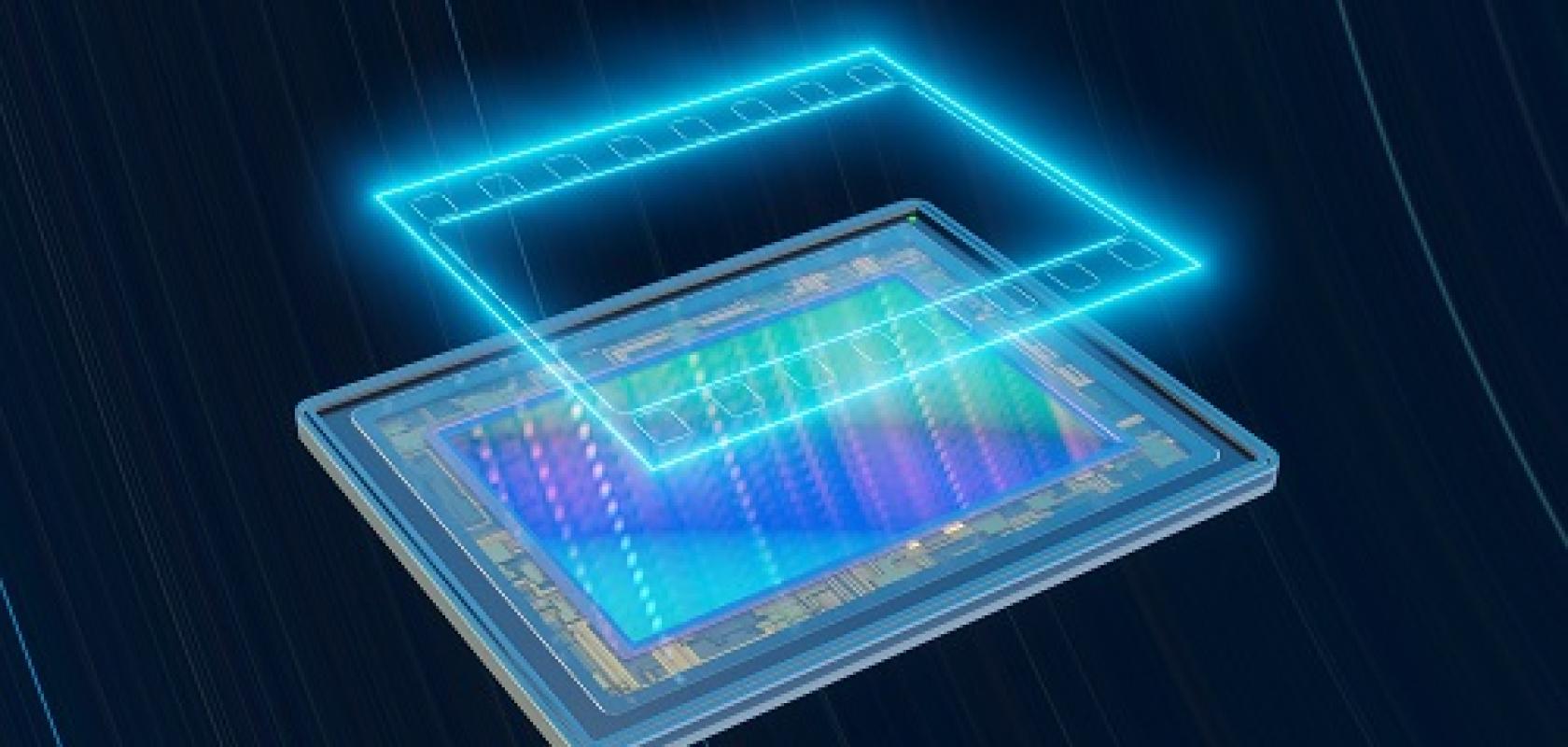
This dramatic expansion will be built upon new forms of sensors, alternatives to the established InGaAs materials. One example are thin-film photodetectors using colloidal quantum dots (QDs) as absorbers, in particular, QDs based on lead sulphide (PbS). Quantum dots were originally developed in the mid-2000s as a solution-processed material capable of competitive sensitivity at wavelengths above 1,000 nanometres. But since their discovery, significant advances in vital real-world parameters such as quantum efficiency have been made.
"Quantum dots are not just a curiosity anymore," comments Pawel Malinowski of Belgian research lab Imec, one centre of development for QDs and their use in SWIR image sensors. "The SWIR market is starting to open up because of certain particular technology developments, of which QDs are one. They are broadband absorbers whose spectral response can be adjusted through stack design and other parameters, and I expect to see further improvements in performance as the technology matures."
Maturity will follow directly from QDs being put to use in the market and developers observing the sensors' performance as they enter real-world applications – a process that is now starting to happen. From there, Malinowski sees three broad use cases taking shape.
One will be the straight replacement of InGaAs sensors by QDs in applications currently using the established technology, although even QD developers acknowledge that the new materials may not necessarily be the best choice for users happy with existing SWIR sensor performance. A second scenario is where better performance actually is the goal, for example in semiconductor wafer inspection where the smaller pixels possible in a QD sensor could lead to a higher resolution image.
Taking the lead
"The third, and for me most interesting, user case is where SWIR has never been used before but now comes within reach," says Malinowski. "New technologies will make investment in SWIR attractive for entirely new uses, and these are the big markets that will then open up."
Meanwhile QD developers at Imec are focusing on ways to optimise the manufacturing and long-term reliability of QD-based sensors and tackling an issue that remains inherent – for now at least – in the technology: its use of lead.
"The volume content of lead is small, typically below 0.1% of the volume, and I think the first QD products will appear where users can tolerate it without a problem," comments Malinowski. "But for some developers and some applications, any lead at all is simply no-go. So, there is already a great deal of research underway into alternative formulations, which might ultimately have even better performance, and in how to make QDs fully fab-friendly and manufacturable."
Malinowski anticipates that all these hurdles will be overcome as SWIR starts to become a go-to technology of choice for certain high-volume uses, and as developers exploit the customisation possibilities that new SWIR sensor materials can offer.
- Imec's Paweł Malinowski on the SWIR imaging landscape from last year
- ST's quantum dot sensor set for volume SWIR imaging
- Emberion’s CEO and CTO, Jyrki Rosenberg and Tapani Ryhänen, about what the future holds for nanomaterial SWIR sensors
"Comparisons with InGaAs are hard, since that is an incumbent technology developed over several decades, and QDs have only seen their first commercial products launched in 2021," he says. "But now it is all about putting QDs to work, studying the reliability, and maximising performance. For quantum dots, all the pointers are in the right direction."
SWIR, meet CMOS
TriEye, an Israeli tech company founded in 2017, has developed high-definition SWIR image sensors that can be manufactured using conventional CMOS semiconductor processes, an approach that drives down the costs of manufacture compared to established InGaAs sensors.
Built on nanophotonics breakthroughs made at Hebrew University in Jerusalem, TriEye production technology is capable of reducing the sensor's pixel size and so boosting the SWIR image resolution, with the company's standard product currently achieving 1,280 x 960 resolution in a CMOS imager format. Just as importantly, the technology fits readily into existing mass-production workflows where CMOS-fabricated devices are familiar items.
"Industrial SWIR imaging today is limited by the cost of InGaAs cameras," comments David Cheskis of TriEye. "Our CMOS-based SWIR technology reduces the cost of the sensor and can be applied in nearly all industrial camera applications. For SWIR applications it allows both cost reduction and mass production."
The company's current CMOS SWIR sensors have somewhat lower quantum efficiency than InGaAs sensors and higher dark current, factors which may limit the technology's ability to replace existing sensors for high-end imaging applications in military or aerospace sectors. But TriEye anticipates CMOS SWIR making its impact in entirely new sectors, expanding SWIR imaging into the higher volume markets identified by Yole.
As well as reducing the costs, TriEye's technology can also add depth-sensing capabilities to SWIR imaging: the company's Sedar (Spectrum Enhanced Detection and Ranging) platform combines SWIR imaging with deterministic 3D depth sensing, by including an illumination source.
"Incorporating illumination is the key," says Cheskis. "Combining the sensor and illuminator into the Sedar platform expands the capabilities of SWIR 3D depth sensing systems to operate outdoors and at long range, while still maintaining eye safety."
Drive my car
On-board illumination also facilitates the incorporation of existing object detection algorithms and machine learning routines, making it easier to identify the objects and people caught on SWIR cameras or the varied materials imaged in a single scene.
Consumer and mobile devices could readily benefit, with Sedar able to enhance the usable range of depth sensing technology on-board smartphones beyond that possible with current non-SWIR implementations. Developers such as Intel and Apple are already familiar with, and employ, near-infrared as a sensor technology in their consumer platforms, and CMOS SWIR could represent the next evolution of that capability for those same devices.

One of the targets for lower cost SWIR sensors is the automotive sector for driver assistance. Credit: Andrey Suslov/shutterstock.com
Another TriEye target is the automotive sector, where autonomous vehicles and advanced driver assistance systems (ADAS) currently employ lidar technology to image the world around them, monitoring the environment and reacting accordingly. TriEye believes that Sedar will reduce the costs of current ADAS platforms by more than a factor of ten.
"These applications are all made possible by the basic principle of a low-cost and high-volume CMOS SWIR platform," says Cheskis. "Ten years ago, a revolution in imaging took place when near-IR and 3D capabilities came to the market, and now a SWIR revolution is beginning. Automotive applications have a longer design cycle than other markets, but there are commercial sectors able to use CMOS SWIR that will deploy the technology as it becomes available. So, we expect to see a lot of CMOS SWIR activity during 2023."
Every photon is precious
The imminent growth in SWIR applications will not stem solely from novel sensor technologies, however. InGaAs sensors remain an established option and well suited for certain applications, while developers with a deep understanding of the material's capabilities continue to enhance its sensing capabilities.
"InGaAs still has a major role to play in the shortwave band," comments Frédéric Aubrun of Xenics, a developer of infrared image sensors originally spun-out from Imec in 2000. "Its combination of sensitivity, signal-to-noise ratio, dynamic range and quantum efficiency mean that for a group of applications there is no real replacement for InGaAs, and there won't be one for some time to come."
Operational performance is the key to this longevity, and Aubrun points to the role that InGaAs can play within the complete ecosystem of industrial SWIR vision systems, where every photon is a precious resource.
Xenics has supplied InGaAs sensors for food sorting and processing lines where frozen items fall through an imaging system's field of view at high speed and under gravity, a scenario in which increasing the illumination power to compensate for a short sensing window would be damaging to the product itself. InGaAs remains the best option for harvesting the available light in this kind of scenario, according to Xenics.
Surveillance and security systems likewise require particular quantum efficiencies from their SWIR sensors, in order to provide acceptable night vision or object detection. The combination of performance parameters that characterise InGaAs sensors can make them more effective for these use cases than newer emerging technologies.
Cost vs capability
Even so, Aubrun recognises the factors that have helped to spur the development of those novel sensors.
"It's true that InGaAs is a relatively expensive technology," he comments. "At Xenics, our response is to master the production of InGaAs sensors from start to finish, controlling the production yields of our own production lines so that we balance costs against manufacturing volumes. As InGaAs applications evolve, we aim to take our products' future under our own control."
One evolving InGaAs business could be free space optics, where the low atmospheric absorption of shortwave wavelengths allows more efficient optical signal transmission than can be achieved with visible light. The trade-off between enhanced transmission and the costs of an InGaAs device will favour the established sensor technology as an economic solution for free space optic communications and quantum key implementations, says Aubrun.
At the same time, the company is engaged in enhancing those established InGaAs properties further, researching ways to control the dark current from the photodiode in the absence of incoming photons, and perhaps modifying the spectral response band of the sensor material itself. These improvements stem from a deep knowledge of the InGaAs material, one built up over decades of industrial use.
"This is not something you can just do in a snap, since it requires an investment of both money and resources," Aubrun adds. "Our product line is evolving, our business is growing, and InGaAs is still a significant sensor technology."