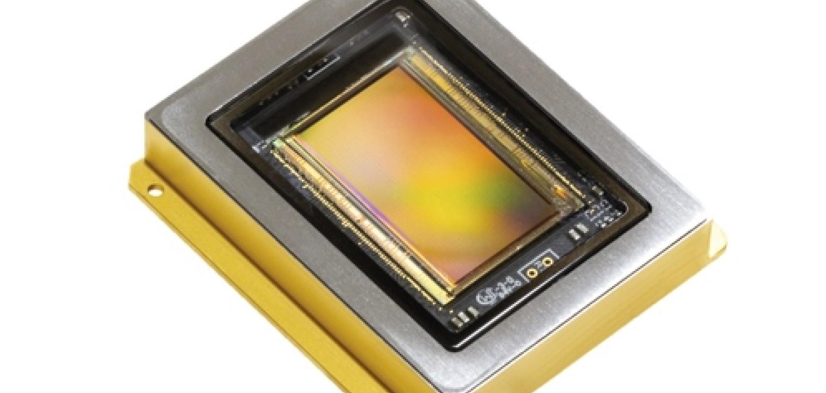
In October, Belgian research institute Imec unveiled a prototype thin-film monolithic image sensor capable of capturing light in both the near infrared (NIR) and shortwave infrared (SWIR) wavelengths.
The sensor consists of a thin-film photodetector pixel stack based on low-bandgap quantum dot materials, deposited directly on top of an electronic readout.
Quantum dot sensor technology – Imec’s sensor is the latest release in this area, but US-based SWIR Vision Systems is now selling its Acuros CQD VIS-SWIR cameras based on colloidal quantum dots – has the potential to lower the price of SWIR imaging substantially.
Pawel Malinowski, Imec’s thin-film imagers programme manager, explained: ‘The advantage of using quantum dots in sensor fabrication is that unlike other processes, you don’t need to grow any material on wafers. Quantum dots can instead be coated onto wafers and then processed through a semiconductor fab in mass-production processes, so this is the big differentiator.’
Currently, the SWIR imaging market is dominated by sensors made with indium gallium arsenide (InGaAs), a semiconductor material grown epitaxially on indium phosphide substrates. In order to form electrical connections between each photodiode and the corresponding silicon readout integrated circuit, the two devices are joined, one detector at a time, by metal-to-metal bonding.
This process, known as hybridisation, is time-consuming, expensive and also imposes limitations on the sensors’ pixel size, pixel spacing and resolution. Because of this, InGaAs cameras are mostly VGA resolution, with only a few exceptions. In addition, because of the cost of their fabrication, these cameras are often considered to be too expensive for most machine vision applications.
The new SWIR imaging solutions based on quantum dots, on the other hand, can be fabricated monolithically on silicon readout wafers, and can therefore take advantage of the scale and cost structure of the silicon integrated circuit industry. Quantum dot SWIR sensors are also able to reach higher resolutions, up to the multi-megapixel level. They therefore have the potential to move SWIR imaging from being a specialised niche into broad commercial markets.
Nanocrystal clear imaging
Quantum dots are nanocrystals that, depending on their size, offer different light absorption properties. For example, particles approximately 3nm in size absorb at 940nm, while particles around 5.5nm in size absorb at 1,450nm. The pixel stacks of the new sensor can be tuned to target a spectrum from visible light all the way up to 2µm wavelength.
‘Right now there isn’t much of a SWIR imaging market, because there is such a high [price] threshold for acquiring a SWIR camera,’ said Malinowski. ‘In a lot of machine vision applications people are not using SWIR because they cannot get a camera, so what we are hoping for is that because we can offer SWIR imaging at orders of magnitude lower price, then new applications will pop up.’

A SWIR image taken of a shoreline, which can be seen clearly through low-visibility rain. Credit: SWIR Vision Systems
Malinowski mentioned agriculture as one area that could benefit from the new SWIR sensors, to use on harvesting robots or for monitoring humidity or moisture. He also believes the sensors could be integrated into smartphone cameras or for applications such as augmented reality. ‘In inspection, they could be used for food or plastics sorting, and in surveillance for low-light cameras with better contrast,’ he said. ‘Additionally, by enabling feature distinction in bad weather or smoke conditions, one can envision firefighting applications and, in the future, advanced driver assistance systems.’
The first generation of Imec’s quantum dot sensor has a resolution of 758 x 512 pixels and a pixel pitch of 5µm. According to Malinowski, however, the second-generation chips, currently being tested, will have a pixel pitch as low as 1.8μm. He noted that the typical pixel pitch of an InGaAs sensor is between 15μm and 20μm.
Despite the lower fabrication cost and higher resolutions achievable with the new sensor technology, Malinowski said quantum efficiency – the performance achieved for the amount of light – will only be around 30 to 40 per cent; InGaAs sensors are able to offer 80 to 90 per cent quantum efficiency. He added: ‘I think that InGaAs will remain unbeatable in terms of high-end performance for the time being. This won’t be same story as CMOS versus CCD, however – there will always be space for both quantum dot and InGaAs sensor technologies.’
Imec aims to have its first wafer-level active NIR and SWIR sensors next year.
Complete cameras
Quantum dot-based SWIR imaging technologies are also available from US-based SWIR Vision Systems, which has been selling its Acuros colloidal quantum dot (CQD) VIS-SWIR cameras from Q3 2018. The cameras are available in VGA (640 x 512 pixels), one-megapixel (1,280 x 1024 pixels), and full HD (1,920 x 1,080 pixels) formats, and as of recently have had a thermoelectric cooler added to the CQD sensors in order to improve their signal-to-noise ratio.
‘Demand for these cameras has been increasing throughout 2019,’ said George Wildeman, CEO of SWIR Vision Systems, who remarked that the 1,920 x 1,080-pixel model, which has a resolution six times higher than the current standard 640 x 512-pixel InGaAs cameras, is the first of its kind to be commercially available. ‘There are a few high-resolution InGaAs cameras with 1,280 x 1,024-pixel sensor arrays, but these are very high cost,’ he said. ‘It is a big challenge to scale InGaAs cameras to larger array sizes without a large increase in their price point.’
One of the primary markets taking advantage of these higher resolution CQD cameras, according to Wildeman, is silicon chip and silicon wafer inspection, where manufacturers want to identify finer defects or cracks in silicon substrates.
The high-resolution SWIR images that can be captured with emerging quantum dot-based sensors can be used to identify defects in semiconductor chip production. Credit: SWIR Vision Systems
Silicon is transparent in the SWIR wavelength band. For example, a bonded wafer pair can be backside illuminated with SWIR light to identify alignment marks and also inspect for void defects. This is not possible in the visible band where silicon is opaque. ‘Our full HD SWIR value proposition is definitely resonating here,’ Wildeman said.
Another application expected to benefit from high-resolution SWIR cameras is maritime imaging, where they can be used to see through haze and other obscuring weather conditions.
In addition, Wildeman expects this technology to be of interest to laser beam profiling, optical alignment, hot glass inspection, liquid fill level measurement and art restoration applications. ‘Wood moisture detection in lumber facilities is also an emerging application for this technology, one that we weren’t originally anticipating,’ he added.
Similar to Malinowski, Wildeman believes that the high quantum efficiency of InGaAs SWIR cameras will maintain the technology’s dominance in high-end imaging applications, in addition to those involving a low number of photons – such as nighttime imaging. However, SWIR Visions Systems has so far found that the combination of its full HD sensor with LED- or halogen-based infrared lighting is able to deliver high-quality images for most machine vision applications.
The firm plans to move to smaller pixel pitches in the future – its first product is designed on a 15µm pixel pitch, but the company has demonstrated sub-3µm pixel pitch in the lab. It will also work to increase quantum efficiency. ‘The quantum efficiency for CQD sensors will not reach 70 per cent anytime soon, so we expect there will always be room for InGaAs cameras, especially in less cost-sensitive applications,’ Wildeman said.
Finally, SWIR Vision Systems is working on cameras with broader bandwidths. Its Acuros cameras already cover the entire visible and SWIR band with one sensor – from 400nm to 1,700nm. It will now extend the bandwidth out beyond 2µm, which, according to Wildeman, will open up new applications, for example in chemical detection, plastic sorting, hyperspectral imaging, methane detection and mineral detection.
Graphene-enhanced detectors
The Acuros cameras will soon be joined on the market by another VIS-SWIR sensor using quantum dots, from Emberion, a firm based in Finland and the UK.
The first product samples of the sensor, which offers VGA resolution, 20µm pixel pitch, 100fps frame rate, and a spectral range from 400nm to 2,000nm, will be available in June 2020.
‘This wide spectral range is the key advantage that our sensor provides over standard InGaAs sensors, which tend to go between 900nm to 1,700nm,’ said Jyri Hämäläinen, director of sales and marketing at Emberion. ‘Beyond 1,700nm is usually called “extended InGaAs”, and it is here that InGaAs technology becomes very expensive. In comparison our sensor is much more affordable while being able to detect these wavelengths.’
Emberion is targeting both monochromatic machine vision and hyperspectral camera manufacturers with the new sensor – particularly those with customers looking to image over a broader spectral range than they can achieve at the moment. ‘We think this sensor will also be interesting to those currently working in the visible wavelength range that are looking to experiment with other wavelengths,’ added Hämäläinen.
While the new sensor will be available as a standalone product, Emberion is looking to offer the technology as a full camera core that includes all the necessary electronics and connections, in order to provide camera manufacturers and integrators a faster and easier way to integrate the technology into their products.
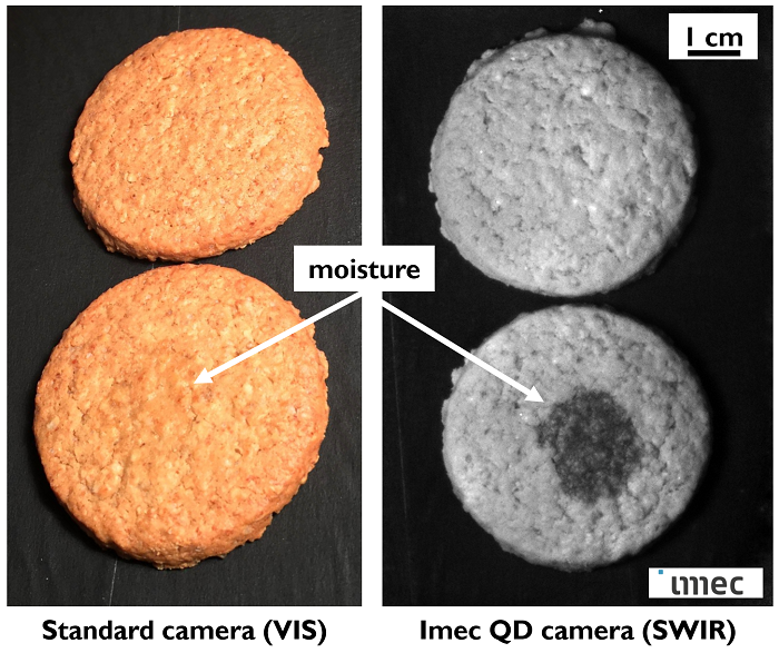
Test images of cookies acquired with a visual sensor (left) and with Imec's quantum dot-based SWIR sensor at 1,450nm (right). The bottom cookie had a drop of water applied to its surface, which can be only distinguished under SWIR light. Credit: Imec
What sets this new device apart from the other emerging quantum dot-based imaging technologies is that Emberion has used graphene to enhance the characteristics of the photodiodes, which significantly increases their sensitivity. ‘Graphene-enhanced photodiodes provide superior responsivity and very low noise,’ said Hämäläinen.
As a partner of the Graphene Flagship programme, a €1bn EU research initiative that aims to transfer graphene from the lab to the market, Emberion has received funding to develop this technology. Hämäläinen remarked that graphene is a new material in imaging, and that he is not currently aware of any other commercial activities that feature graphene being used in machine vision sensors.
Depending on the customer feedback Emberion receives following the release of its technology, the firm may choose to develop its sensor towards higher resolution. ‘Megapixel resolution might be an option, but this will depend on the customer demand,’ Hämäläinen said. ‘We will also be looking at increasing the speed and even further widening the spectral range if this is what is needed from end-users.’
With the sensor’s ability to detect beyond 1,700nm, it could be applicable to plastic sorting applications, which have spectral peaks in this region. In addition, the hydrocarbons in certain foods also have spectral peaks here, meaning the sensor could also have applications in the agricultural industry. ‘While these applications could use extended InGaAs technology, the large cost associated with this often leads to end-users finding alternative solutions that work around this,’ commented Hämäläinen. ‘Our sensor could therefore enable these end-users to address these applications without needing a work-around. We have seen that there is definitely interest here.’
As an additional project, over the next few years Emberion will also be working on developing a broadband imaging sensor – covering everything from visible light to the longwave infrared. According to Hämäläinen, initial research prototypes for this technology already exist. ‘We believe this will bring a totally different dimension to imaging, including new opportunities in machine vision,’ he remarked. ‘We are looking to hear from companies who would be interested in this technology so they can tell us what they need, and then we can steer our development towards achieving the required specifications.’
A new take on shortwave infrared LEDs
In a three-year research project conducted with the French Institute of Optics, machine vision lighting firm Effilux, also from France, has developed an LED SWIR source that it says addresses the drawbacks of current SWIR LEDs on the market.
Arnaud Mestivier, sales manager for Effilux, explained that despite the advantages of LEDs – long lifetime, robust, and less heat dissipation – those that provide SWIR illumination deliver less power and are more expensive than standard LEDs. While visible LEDs deliver around 1W of optical power, SWIR LEDs only offer approximately 20mW to 50mW. The cheapest solution for SWIR illumination capable of delivering the most optical power was therefore previously halogen bulbs, according to Mestivier, which deliver 100 times more optical power than SWIR LEDs.
Now, however, as a result of the research project, Effilux and the French Institute of Optics have developed the SWIR High Optical Power LED source. According to Mestivier, the technology retains all the advantages of LEDs compared to halogen bulbs, while also offering considerable improvements in power, as well as the flexibility to create both highly focused SWIR beams and large area uniform SWIR illumination.
The new source uses low-cost LEDs emitting at 940nm to pump a crystal that re-emits at 1,550nm, which – for a similar price – produces 10 times more light than a 1,550nm SWIR LED. In addition, Mestivier said that one chip of the technology is able to emit a luminous flux comparable to a 50W halogen source. As a result, many expensive SWIR LEDs can now be replaced by a single SWIR High Optical Power chip, resulting in lower costs for system builders using SWIR illumination.
The LED chip offers approximately 50,000 hours of operation, high stability and reliability, quick pulse operation, compact size, no excessive warm up, and low power consumption. It is also fully eye-safe.