Late last year Imec presented a shortwave infrared quantum dot image sensor with a pixel pitch of 1.82µm at the IEEE International Electron Devices Meeting (IEDM).
The work is the latest in several advances in SWIR image sensor technology, which have been gathering pace where, previously, progress in III-V detectors had ground to a halt. A year earlier at the previous IEDM, Sony announced SWIR sensors with a 5µm pixel pitch, achieved by connecting the InGaAs photodiode to the readout circuit via copper-to-copper bonding. This meant that, finally, the limitation of double-digit pixel size found in traditional hybrid bonded InGaAs sensors was broken, offering a path to higher resolution SWIR sensors.
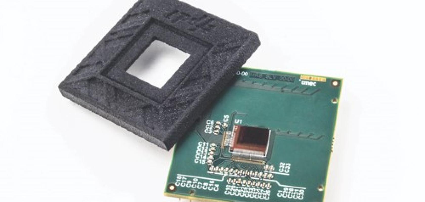
The Imec sensor is based on thin-film quantum dots, which are integrated monolithically on top of the readout circuit. This means it doesn’t have the limitations of flip-chip bonding or interconnects, so the pixel can be very small – 1.82µm is the smallest pixel Imec has made with this particular technology node of 130nm in a three-transistor (3T) structure.
‘We want to have small pixels, which is good for image quality but also for squeezing more pixels in the same footprint,’ explained Paweł Malinowski, program manager for pixel innovations at Imec. ‘This translates to lower cost per pixel.’
Malinowski said the sensor could one day be manufactured in the €10 to €100 range, once larger volumes are possible – current InGaAs sensors can cost a few thousand euros. He said that at this early stage €100 or €200 is adequate for most customers.
Quantum dots can be engineered to have absorption at 2µm and above. The absorption peak can be tuned to certain wavelengths by the way the thin-film layers are constructed. In the IEDM paper, Imec focuses on sensing at 1,450nm, a useful detection wavelength for some applications, especially if water content is a desired metric.
A quirk of designing image sensors with quantum dots, Malinowski noted, is that the quantum dot absorber layers, at 300 or 400nm thick, are significantly thinner than the wavelength of light they are used to detect, 1,450nm. ‘From a physics point of view, it’s quite amazing,’ he said.
Imec has reached around 50 per cent external quantum efficiency (EQE) on test structures, while on ROIC samples EQE is currently 10 to 20 per cent. InGaAs reaches up to 80 to 90 per cent EQE, so quantum dot sensors won’t compete where high quantum efficiency is needed, but for a lot of applications, 50 per cent EQE is acceptable, Malinowski said.
Complete package and new applications
The announcement is the result of several things coming together: the optimisation of the photodiode for the infrared range; designing a circuit that can read out the signals from such a thin-film photodiode – typically these materials have higher noise or higher dark current, so the photodiode has to cope with that; and all the necessary integration, the interconnects, and how the sensor is encapsulated and packaged.
Imec is now working on transferring the process to its 200mm fab and making the devices on full wafers. Once that is available, throughputs will be higher and the device can be optimised for uniformity and reliability.
Malinowski said that the first applications might be for areas in industrial vision requiring higher resolution in SWIR, for instance inspecting solar cells or silicon chips. Higher resolution means the field of view can be increased.
Smart agriculture is another area that he highlighted. He said that agricultural robots don’t use SWIR sensors at the moment because they can cost more than the robot itself, so a less expensive SWIR imager might open the door to more widespread use of SWIR in agriculture.
The example given in the IEDM paper is inspecting structures through silicon using lens-free imaging, a type of microscopy where the image is reconstructed computationally. Here, there is an advantage of having a large field of view and sub-wavelength pixels in the shortwave infrared. ‘The new sensor is an enabler, because right now lens-free imaging for SWIR is quite difficult,’ Malinowski explained.
A bit further off, the SWIR sensors could potentially be used onboard cars – although automotive has strict requirements in terms of reliability – and also in consumer devices. The cost would need to drop even further, but one potential application is in VR glasses for eye tracking at 1,500nm.
To reduce the price point further, the sensor would have to be manufactured on 300mm wafers, which would allow pixels to be scaled down even more and additional functionality added.
Imec is also considering making a multispectral sensor, to incorporate different absorbers for different pixels or pixel regions.
Malinowski said that the priority at the moment, however, is using just one type of absorber for a straight SWIR sensor.
Optimising on 200mm wafers
Peak absorption in the 1,450nm sensor detailed in the IEDM paper has a full width at half maximum of around 100nm. The detector has a sensitivity profile of 60 to 70 per cent sensitivity in the visible spectrum, which drops to 10 per cent between the visible and the peak in SWIR, with the peak optimised to a maximum of around 50 per cent EQE.
‘It’s a pretty broadband detector,’ Malinowski said. ‘If you want to use it with a light source of a certain wavelength this is where you want to optimise the peak. If you want to capture as much light as possible, all the wavelengths between the visible and the peak are usable.’
At the moment Imec is working at room temperature, but there are tests to see the effects of operating at higher or lower temperatures.
‘We keep on optimising the stack and working with material suppliers to explore new materials,’ Malinowski said. ‘Going lead-free is a big topic.’ At the moment, Imec’s baseline technology is lead sulphide quantum dots, but some companies have a strict lead-free policy. Indium arsenide is another potential material, he said.
‘This is not a technology that will substitute or take away market from traditional SWIR imagers,’ Malinowski added. ‘This is filling the gap between the silicon image sensors and the InGaAs or III-V for applications that can’t afford SWIR, or that need higher resolution than that available in flip-chip sensors.
‘I see this technology as a new thing, rather than a competitor. InGaAs will always be preferable for high-end SWIR imaging, where you need the highest efficiency.’
Progress is being made in this area from other companies too, notably SWIR Vision Systems in the US, with its Acuros quantum dot SWIR sensors and cameras, and Finnish firm Emberion, which is working on integrating graphene and other nanomaterials onto CMOS integrated circuits for broadband detectors. In addition, Spanish research institute ICFO last year spun out Qurv Technologies to develop quantum dot image sensors operating from the visible to the shortwave infrared.
‘There’s quite a lot of movement disrupting the SWIR market, which has for decades been made up of traditional players,’ Malinowski said. ‘We are at an interesting point in time, and we hear from integrators and application companies that they want to have SWIR. I’m optimistic for the future.’
Commercial products
Gpixel has announced the first sensor in a new family of CMOS line scan imagers supporting true charge-domain time delay integration (TDI). GLT5009BSI is a backside illuminated, TDI image sensor with 5µm pixels and 9,072 pixel horizontal resolution. The sensor has two photosensitive bands, 256 stages and 32 stages respectively, enabling a high dynamic range imaging mode.
The sensor’s 5µm pixel provides a full well capacity of 16ke- and noise of 8e- which delivers 66dB dynamic range. The GLT sensor family employs scientific CMOS BSI technology to achieve excellent sensitivity from the ultraviolet to the near infrared.
Read out of the image data is achieved through 86 pairs of sub-LVDS channels at a combined maximum data rate of 72.58Gb/s. This output architecture supports line rates up to 600kHz using 10-bit single band mode, and 300kHz using 12-bit single band mode.
The length of the photosensitive area is 45.36mm and the sensor is assembled in a 269-pin µPGA package. The sensor integrates several features to ease camera integration, including an internal sequencer, channel multiplexing, and selectable scan direction.
The GLT family’s combination of high speed and sensitivity from the UV to the NIR, is ideal for applications such as flat panel display inspection, printed circuit board inspection, wafer inspection, digital pathology and fluorescence imaging.
Other recent image sensors from Gpixel include: GMax2518, a global shutter, 18 megapixel sensor with correlated double sampling and an optical format of 1 inch; GSprint4521, a 21 megapixel APS-sized sensor designed with 4.5μm charge domain global shutter pixels; and the 103 megapixel GMax32103 medium-sized sensor with a 3.2μm global shutter pixel.
Elsewhere, foundry Tower Semiconductor and Opix, a supplier of time-of-flight sensors, have developed a ToF technology platform for 3D imaging and face recognition. The technology is implemented in a high-end image sensor product that is being integrated into a 3D camera module in partnership with a provider of imaging systems for mobile applications. The product will serve a variety of markets such as mobile, AR/VR, retail, robotics, automation and industrial inspection.