As semiconductor manufacturing moves towards smaller geometries, advanced packaging and increasingly complex architectures, the ability to detect what conventional cameras cannot see is becoming a critical part of the production process. At SEMICON West 2026, Exosens will showcase a broad portfolio of advanced imaging technologies, spanning ultraviolet, visible/NIR, SWIR and long-wave infrared.
The company’s focus is not a single product launch, but a wider proposition: matching the right imaging technology to the physical phenomena that semiconductor manufacturers need to detect, measure and understand.
Taking place at the Moscone Center in San Francisco, USA, from 13 to 15 October, SEMICON West is, of course, a major meeting point for the semiconductor manufacturing ecosystem. Its importance to photonics and imaging companies lies in the way it brings together chipmakers, equipment manufacturers, process engineers, technology developers and suppliers working across the production chain. For Exosens, this makes the event an opportunity to engage with the people defining inspection requirements, rather than simply presenting camera specifications.
The show’s 2026 programme reflects changing industry priorities. Under the theme Transform Tomorrow, the event will examine the technologies and investments shaping semiconductor growth. Its agenda covers advanced manufacturing, AI and next-generation computing, supply chain resilience, sustainability and semiconductor infrastructure.
The Exosens message for SEMICON West is straightforward: as semiconductor manufacturing becomes more complex, the ability to see beyond the visible becomes increasingly critical. “SEMICON West’s 2026 programme puts strong emphasis on advanced packaging, metrology and inspection, AI-enabled manufacturing, thermal management and silicon photonics,” says Marc Larive, Director of Business Development. “Our message is therefore simple: as semiconductor manufacturing becomes more complex, the ability to see beyond the visible becomes increasingly critical.”
The company’s focus at the show will be on demonstrating the breadth of its advanced imaging portfolio, covering wavelengths from ultraviolet through visible/NIR and short-wave infrared to long-wave infrared. That breadth is important because semiconductor inspection is not one application. A surface defect, a subsurface feature, photon emission and a thermal anomaly may all require different approaches to imaging, and a camera that performs well in one part of the spectrum may not be suited to another.
Exosens stresses buying decisions are complex: it cannot just be about the camera that happens to be available. “Ultimately, we want customers to see Exosens not simply as a camera supplier, but as a technology partner capable of addressing different imaging challenges across the semiconductor manufacturing process,” says Larive.
UV imaging for wafer inspection
At the shorter-wavelength end of the portfolio, Exosens offers UV imaging from approximately 190 to 400nm. UV imaging can be particularly valuable for applications where conventional visible imaging does not provide sufficient contrast or sensitivity. Exosens identifies dark-field wafer inspection, defect and residue detection, mask inspection and other difficult-to-observe phenomena among the relevant applications. For semiconductor manufacturers, that can mean improving the ability to identify defects and variations at points in the manufacturing process where early detection is important. The company will use SEMICON West to demonstrate how this capability fits within a wider inspection strategy, rather than treating UV as an isolated technology.
The company’s SWIR portfolio is built around InGaAs cameras, addressing applications including wafer and die inspection, photon-emission microscopy and silicon ingot inspection. The longer wavelengths available in SWIR can provide visibility into defects and structures that are not accessible using visible imaging. This makes the technology relevant to several semiconductor applications where the material being inspected, or the phenomenon being measured, requires a different spectral response.
Exosens’ SWIR offering includes the Wildcat+, Cheetah+, Bobcat+, Manx and Lynx families. These products address different combinations of speed, sensitivity and resolution. The product roster is intended to give customers options according to their application requirements. A high-speed inspection system, for example, may have different priorities from a low-light photon-emission application or an inspection task requiring higher spatial resolution.
The company’s differentiation is therefore not necessarily one headline specification: it is the ability to select the right spectral technology for the physical phenomenon that needs to be detected and to combine high sensitivity, speed, resolution and reliability according to the application. This is a significant distinction for semiconductor equipment developers, who may be integrating imaging into complex systems rather than buying a camera as a standalone component.
At the opposite end of the spectrum, Exosens will highlight its long-wave infrared cameras, including the Ceres T series. Thermal behaviour is becoming an increasingly important consideration in semiconductor manufacturing, particularly as advanced packaging, higher power densities and more complex architectures introduce new thermal-management challenges. The 2026 SEMICON West agenda reflects this, with dedicated programming on thermal management in advanced packaging and testing. Exosens’ LWIR cameras enable thermal inspection and monitoring of wafer manufacturing processes. The company identifies the detection of thermal defects and the assessment of temperature uniformity as key applications.
The relevance of thermal imaging is that temperature can provide information about a process that is not necessarily visible through conventional imaging. By capturing thermal behaviour, manufacturers can investigate variations and identify issues that may otherwise remain hidden. As with UV and SWIR, the value lies in selecting the appropriate imaging approach for the physical problem.
A broader technology base
Exosens’ proposition is underpinned by more than 85 years of experience in high-end electro-optical technologies, with expertise spanning amplification, detection and imaging. The company’s imaging portfolio covers a broad spectral range, from UV below 300nm through visible/NIR, SWIR, MWIR and LWIR. It has R&D and production sites across Europe and North America, and more than 2,000 employees globally.
The breadth of the portfolio is supported by complementary technologies and acquisitions. Exosens highlights the integration of Emberion’s quantum-dot SWIR sensors and Phasics’ optical metrology expertise as part of its efforts to address increasingly sophisticated industrial and semiconductor imaging requirements. For semiconductor customers, the attraction is the opportunity to access a wider technology base while working with specialists on demanding imaging problems. That is particularly relevant as inspection and measurement requirements evolve alongside the semiconductor industry. The question is not always which camera offers the highest resolution or fastest frame rate, but which combination of spectral response, sensitivity, speed and reliability can deliver useful information from the process.
At SEMICON West, Exosens wants to move the conversation beyond a conventional equipment-buying question. “Our ambition is to move the conversation beyond ‘what camera do you need?’ toward ‘what do you need to see, measure or detect?’,” says Rosa Maria Vinnella, VP of Products. That shift reflects the breadth of its portfolio and the range of applications it is targeting. Whether the challenge involves a surface defect, a subsurface feature, photon emission, material variation or thermal behaviour, the company argues that the relevant starting point is the information required from the process.
As the industry moves towards advanced nodes, heterogeneous integration, AI-driven production and more demanding inspection requirements, Exosens believes that seeing beyond the visible can contribute to better inspection, process control and, ultimately, higher manufacturing performance.
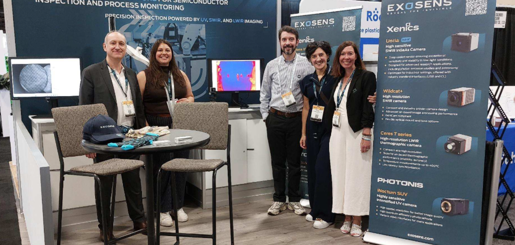
The company will be exhibiting at SEMICON West, 13 to 15 October, at the Moscone Center in San Francisco. Visit Exosens at Booth 6752.