
Five companies are competing for the 2026 VISION Award, with the winner to be revealed at the VISION trade fair in Stuttgart this October. From coherent 4D sensing to configurable SPAD architectures, the shortlist reflects the breadth of approaches now pushing industrial vision beyond conventional 2D and 3D imaging. Here, we take a look at each of the five finalists and the innovations putting them in contention.

PHOTODEX combines photometric stereo and automatic CAD-based localisation in a single, portable system (Image: Austrian Institute of Technology)
Austrian Institute of Technology (AIT)
PHOTODEX: a mobile inspection system for intelligent, robust industrial surface analysis
PHOTODEX, developed by the Austrian Institute of Technology (AIT), is a portable industrial inspection system that enables high-resolution surface inspection during continuous handheld or robotic operation.
Its key innovation is the combination of motion-robust, quasi- single-shot photometric stereo and automatic CAD-based localisation in a single portable system. As a result, manufacturers can perform reliable high-resolution inspection without motion artifacts, while every detected defect is automatically registered to its exact position on the digital twin. This helps manufacturers detect surface defects faster, reduce inspection costs, minimise scrap and rework, and generate standardised, spatially referenced AI-ready ground-truth datasets.
Unlike conventional inspection systems, PHOTODEX maintains full spatial resolution during continuous scanning, making it ideal for inspecting large or difficult-to-access components. By automatically registering every detected defect to its exact CAD model position, the system creates structured inspection data that integrates directly into digital engineering and quality management workflows.
This unified workflow for surface characterisation, defect localisation, and digital quality assurance enables applications in the automotive, die-casting, battery manufacturing and aerospace industries, improving productivity, defect traceability, root-cause analysis and AI-driven quality assurance.
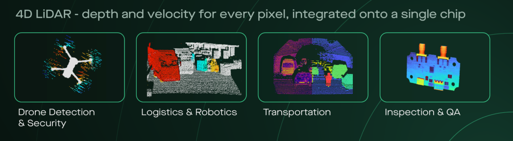
Lidwave's 4D lidar optical chip – depth and velocity for every pixel (Image: Lidwave)
Lidwave
Odem: 4D coherent vision on a single chip
Odem is the world's first and only single-chip 4D lidar – the perception layer for physical AI. It gives robotics and drone makers, automotive OEMs and Tier-1s, industrial-automation firms, and smart-city and security operators one sensor that measures range and per-pixel velocity together, in a single frame and in any condition.
That turns perception from reactive to predictive: not only where objects are, but how fast and where they move – separating moving hazards from static clutter instantly, with total immunity to sun glare, ambient light, and cross-talk, as well as clear vision through rain, fog, dust and snow.
The breakthrough is Lidwave's patented finite coherent ranging (FCR), reading the coherence of light rather than its speed. This puts the whole optical engine on one silicon photonics chip in a true monostatic design: calibration-free, built at wafer scale, and streaming millions of points per second over hundreds of metres.
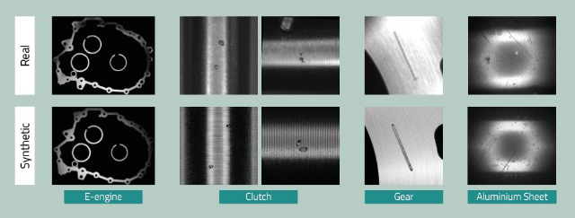
Medabsy's software 'uses physically accurate light transport simulation and mathematical models of textures and defects to create every image'. (Image: Medabsy)
Medabsy
Virtualising machine vision
Our software enables users to virtually design complete machine vision systems using real, commercially available cameras, lenses, lighting, and other hardware. These virtual designs can be then used to generate photorealistic synthetic training datasets with pixel-perfect annotations.
Unlike synthetic data solutions that rely on generative AI, our platform uses physically accurate light transport simulation and mathematical models of textures and defects to create every image. This approach ensures full physical accuracy, complete controllability and realistic sensor behaviour, while enabling users to systematically generate edge cases and apply domain randomisation.
The result is high-quality synthetic data that supports the development, validation, and optimisation of machine vision systems with greater confidence, reduced cost, and faster time to deployment.
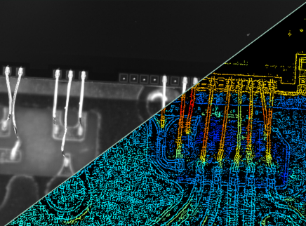
A single photonicSENS apiCAM shot, split to show both outputs: the 2D image (left) and the corresponding calibrated depth map (right), captured simultaneously from one sensor. The colour gradient on the depth side reveals wire bond height and shape with sub-10 micron precision, data a standard 2D camera cannot provide. (Image: photonicSENS)
photonicSENS
From plenoptic research to industrial 3D vision
photonicSENS has turned plenoptic (light field) imaging, understood in theory for over a century, into a manufacturable industrial technology. Its apiCAM platform captures a full 2D image and a calibrated, per-pixel 3D depth map simultaneously, from a single sensor, in a single shot, with no projector, no scan axis, and no on-site calibration.
A Micro-Lens Array between lens and sensor captures multiple angular perspectives in one frame. A proprietary algorithm then extracts genuine, measured depth in real time, including on specular metallic surfaces and transparent substrates that challenge structured light, laser triangulation, and stereo vision.
Manufactured at industrial scale using a proprietary automated alignment process in photonicSENS’ own cleanroom in Valencia, Spain, the portfolio now spans over 50 off-the-shelf camera designs, with depth precision reaching under 0.5 µm at the high end and up to the millimetre range at the other.
Light field imaging has been discussed in machine vision for two decades. photonicSENS is the company that made it a product.
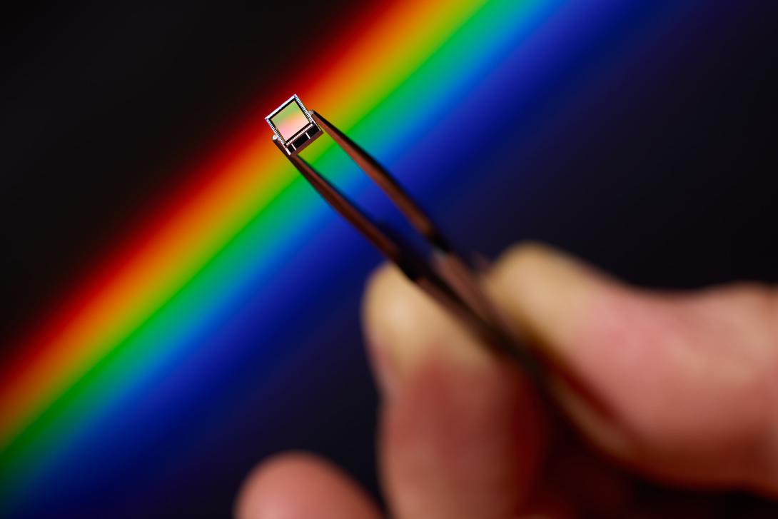
Singular Photonics’ Litavis image sensor (Image: Singular Photonics)
Singular Photonics
Litavis: a software-configurable SPAD image sensor
Coming soon from Singular Photonics, Litavis is a next-generation single-photon avalanche diode (SPAD) image sensor that brings unprecedented flexibility and intelligence to advanced imaging and machine vision.
Unlike conventional sensors, which are typically designed for a single operating mode, Litavis features a software-configurable architecture that combines high-sensitivity photon-counting imaging, programmable time gating and advanced photon timing on a scalable SPAD platform. By integrating embedded digital photon processing directly on the sensor, it enables simultaneous photon-counting and time-resolved sensing for applications including machine vision and lidar, while allowing sensor functionality to be reconfigured in software without hardware redesign.
Processing photon events on-chip dramatically reduces data transfer requirements, enabling lower latency, reduced power consumption and faster real-time decision-making. The software-defined approach transforms image sensors into intelligent sensing platforms that extract meaningful information directly at the focal plane, accelerating application development while reducing system complexity and opening new possibilities for computational imaging.
The winner will be announced at the VISION Award session on Wednesday, 7 October, 2026 at Industrial VISION Days (Alfred Kärcher Halle (Hall 8), 8C70) from 11am-12pm