Currently, machine vision still predominantly relies on the frame-by-frame extraction of data from all the pixels on an image sensor, with conventional RGB imaging systems having to capture everything from the scene (both dynamic and static) in each frame.
Though this can prove effective in many circumstances, there are now times when this is actually becoming seriously problematic. The rate at which imaging data can be required and the bandwidth restrictions associated with certain applications are not well matched with a frame-oriented approach.
The use of machine vision in an industrial IoT (IIoT), robotics or smart city contexts is likely to place acute constraints onto the implemented imaging systems, as well as often requiring accelerated responsiveness. Because of such factors, there is now a clear need to reduce the data communication overheads involved – which means that imaging technology needs to be redefined.
To do this, the optoelectronics sector has taken inspiration from the natural world.
Changing machine’s visual perception
Through the recent emergence of event-based imaging, there is the prospect of making data acquisition procedures much more streamlined. Offering an alternative to the data-intensive frame-by-frame image capture, it is enabling applications in which there are low bandwidth or short latency times to be better addressed. Whereas traditional machine vision has evolved from film photography origins, and therefore mandates complete frame capture, event imaging applies the same basic principles as those used in the vision of humans and animal species.
Humans don’t have large bandwidth channels via which visual data can be transferred. Rather than having to keep on constantly refreshing the whole visual scene, our eyes just inform our brains of any changes that are occurring. Employing the same arrangement to machine vision will result in greatly reduced data volumes and faster updating – and that is the motivation behind event-based image sensing.
Benefits of event-based vision
There are a multitude of situations where event-based imaging is going to be advantageous. Among these are the automated guided vehicles (AGVs) moving through factories and warehouse facilities. By projecting structured light patterns onto an object of interest, it is possible to undertake high-precision depth sensing – with any pattern distortions that occur being determined right down to less than mm-accuracy at speeds surpassing 100Hz. Having less data-heavy imaging hardware will lower the processing required for collision avoidance purposes. 3D movement tracking is another important task – so robot arms can pick items off conveyor belts. Additional tasks worth mentioning are automated palletising, parcel sorting, high-speed item counting, etc.
As less data is generated by event-based imaging, the artificial intelligence (AI) aspect accompanying it can be streamlined – with reduced investment needed in computational resources and less complex stacks being featured. There is also the potential to curtail the level of training required by associated AI algorithms, as the data will already be in a simplified form that is easier for these algorithms to work with. Event-based imaging has value from a public privacy perspective too. By using it instead of RGB camera systems, smart city applications will be much better able to respect people’s anonymity.
A new paradigm
Sony is successfully unlocking the true potential of event-based imaging. It is able to deliver the data needed for high-speed, low-latency examination of phenomena that would have been impractical via standard frame-based systems using its innovative event-based vision sensor (EVS) devices. Here, emphasis is placed on perception of luminance alterations within a scene – so the tracking of movements and determining of vibrations can be achieved without requiring large amounts of computational power.
Each pixel is comprised of a light receiving unit and luminance detection unit. Photons incident on the light receiving unit are converted into a voltage. Then the differential detection circuitry determines if there are any changes (positive or negative) between the voltage generated by the incident light and the reference voltage. If the change experienced is outside a certain predefined threshold value in either direction, then an event is triggered by the comparator and data is subsequently output. Any value that remains within the threshold will be deemed as not having adequate relevance (such as background noise) and will be ignored. The positive/negative threshold settings can easily be adjusted in line with specific application requirements and the ambient environment. For any pixel where a notable luminescence change has been experienced, the EVS will then output the exact coordinates, and the polarity of the change (from lighter to darker or vice-versa). To ensure that events are registered in line with when they occur, timestamping is applied to data before being output from the EVS pixels. Timestamped data is passed into arbitration circuitry, which controls the output order based on the earliest received event.
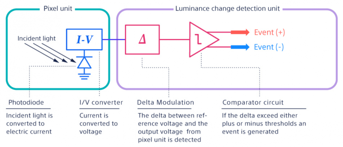
Figure 1: The steps in the event-based imaging process
So that the EVS can keep picking up more data, the circuit associated with each of its pixels is instantly reset after registering an event, with that event’s luminance becoming the new reference value. The positive/negative thresholds are then updated accordingly.
There is provision for tuning the EVS if it is not picking up enough data (or conversely if it is deemed to be picking up too much). Thresholds can also be configured dynamically, should ambient conditions be expected to alter over the course of a 24-hour period. For example, in smart city monitoring applications, diurnal changes in the background illumination may mean the thresholds applied need adjusting.
EVS can be used in places where other imaging systems would not be applicable, due to dynamic range limitations. Incident light luminance is converted into a voltage logarithmically. Consequently, small differences can be picked up in low-light conditions, and conversely, large luminance differences can be addressed in high-luminance scenarios without saturation concerns.
Innovation at the pixel level
In contrast to competing event-based image sensors, Sony’s EVS devices have several key properties that differentiate them. The most important of these is the stacked arrangement employed. Normally the light-receiving and luminance detection elements of event-based image sensor pixels are all on the same layer. This leads to several problems though, as the active area is lost (illustrated in Figure 2).
For the Sony EVS architecture, these elements are incorporated into different layers – so they are stacked one on top of the other, not situated side-by-side. Each light-receiving part of the pixel (on the upper layer) is complemented by a logic element (on the lower layer) with built-in signal processing capabilities. The upshot has less dead space on the pixels. As well as attaining higher resolution, superior low-light performance is also achieved, as more photons can be captured by each pixel. It also facilitates improvements in latency, with the time taken to read respective pixels shortened (as it is quicker to route the data off the image sensor). Since almost all of Sony’s image sensors (not just its EVS ones) have this stacked construction, economies of scale allow the advantages to be realised without adding to the costs involved.
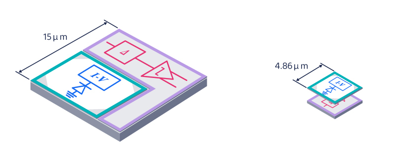
Figure 2: Comparison between a single layer event image sensor pixel and Sony’s stacked EVS pixel
To date, two EVS devices have been introduced by Sony* – namely the 0.92Mpixel, 1/2.5 format IMX636 and the 0.33Mpixel, 1/4.5 formatIMX637. Both have pixels with4.86μm x 4.86μm dimensions – making them the smallest of any event image sensor currently on the market. These sensors have a <100µs temporal resolution and support a 2.3Gevents/s maximum event rate, which means they can analyze GHz vibrational activity. They have an exceptional 86dB dynamic range, thereby giving them broad application versatility.
Sony’s EVS image sensors are causing a major disruption in the global optoelectronics market. There are a multitude of different industry sectors where these devices are already showing their credentials. Among them are the vibration monitoring of industrial equipment (to assist with predictive maintenance), the identification of abnormalities in machinery operation, the control of robot movements, product line inspection, user interface development, edge-located parametric monitoring, plus various forms of machine tending.
Adoption of event-based vision
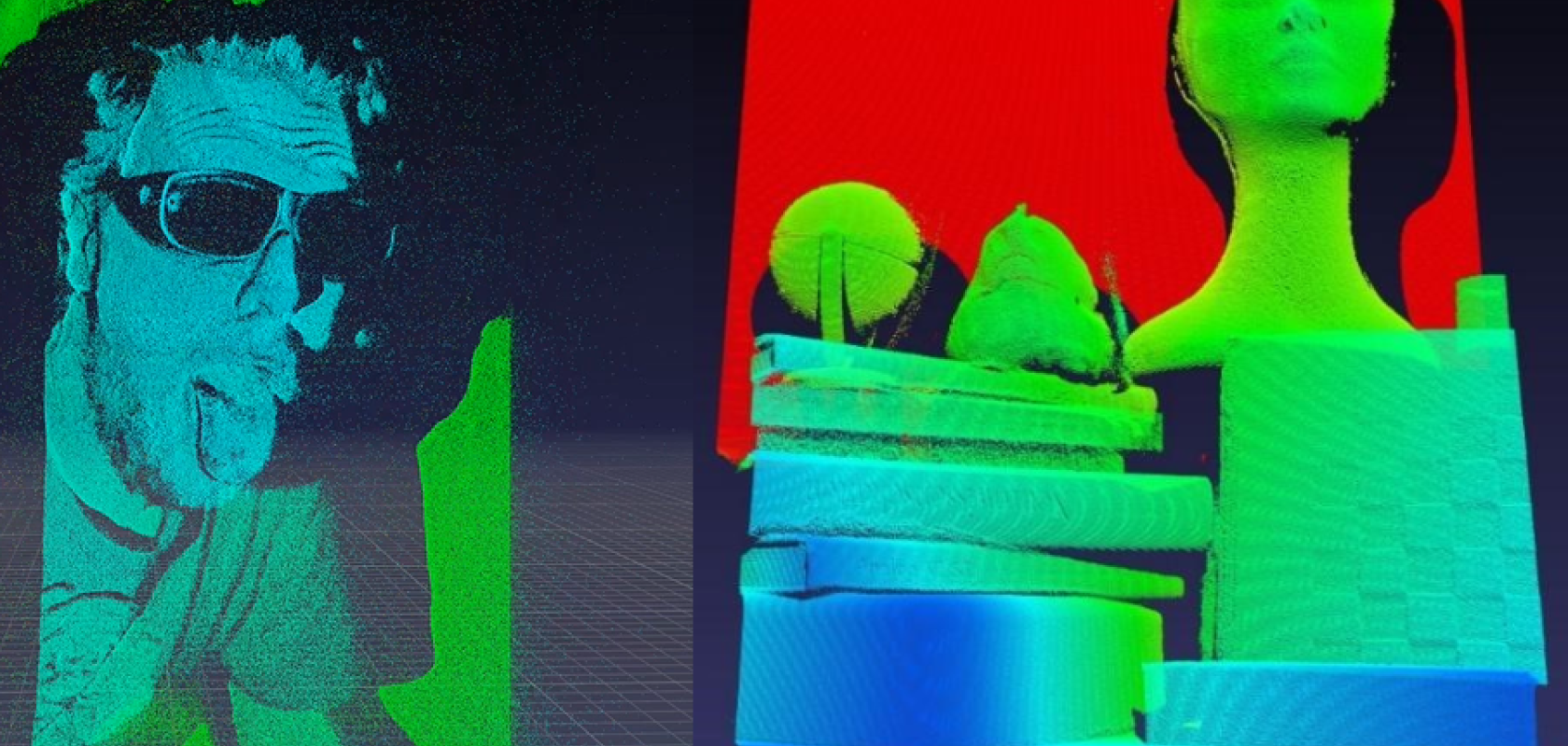
Recent high-speed applications include the monitoring of sparks generated during the metal grinding process. EVS enables analysis of high-speed spark scattering, which RGB sensors struggle to capture because sparks are not visible due to over-exposure. Another high-speed application includes droplet monitoring to prevent defects through better control of the injection and application conditions of liquid and fluid substances. EVS measures droplets to capture changes in speed and shape in liquid and fluid substances. In this case, frame-based RGB sensor data can capture the substance as a fluid but does not convey the droplet condition.

Frame-based RGB sensor (left) for droplet monitoring captures the substance as a fluid, but does not convey the droplet condition, while EVS data (right) measures as droplets to capture movement and changes in shape
EVS technology is also used in 3D measurement applications to improve the signal readout speed of laser triangulation and achieve high-speed 3D measurement. Here, a distinct advantage of EVS over other techniques is that high-speed laser line extraction only takes place when changes occur, increasing the scan rate. A recent EVS structured-light proof of concept was established for industrial sensing to test capabilities in terms of accuracy, precision, speed, and robustness to varied environments. The results showed high temporal resolution, low power consumption, and resistance to motion blur, with submillimeter accuracy and precision in-depth measurements – therefore holding significant potential applications in industries such as robotics.
Conclusion
As we have seen, conventional image capture methodologies have significant drawbacks. They rely on the compiling of data from all of the pixels in the image sensor for each frame. By replacing a frame-based arrangement with an event-based image sensor that mimics the human eye, the resource restrictive demands being set by modern machine vision applications can be attended to – with high-speed imaging data acquisition accomplished, while simultaneously curbing processing and communication requirements. Image systems will be able to do more pre-processing work at source, so data is already in an acceptable format for applying AI algorithms and workloads are made more efficient. Furthermore, selecting an event-based imaging system utilising Sony’s stacked construction permits additional plus points to be derived – with augmented optical and temporal resolution exhibited, alongside extended dynamic range.

Tomohiro Takahashi is the Senior Manager for event-based vision business development at Sony Semiconductor Solutions
Dr Tom Jellicoe is the Product Manager for event-based vision & time-of-flight sensors at Sony Semiconductor Solutions
* IMX636 and IMX637 were made possible through a collaboration between Sony and Prophesee, by combining Sony's CMOS image sensor technology with Prophesee's unique event-based vision sensing technology.