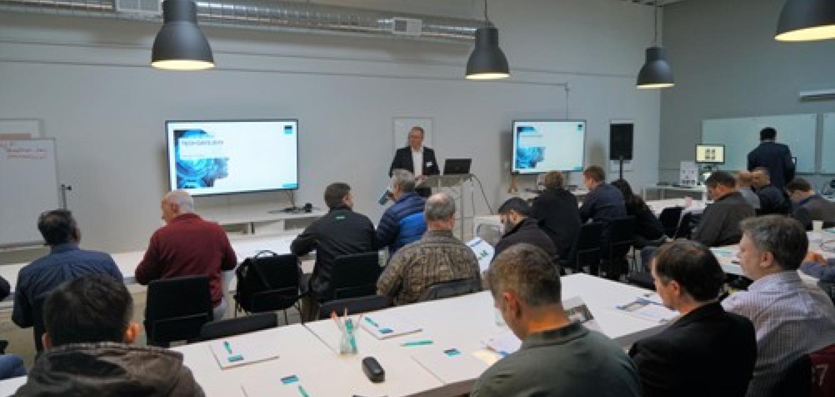
Ron Low, Framos head of sales Americas and APAC, reports from the Framos Tech Days at Photonics West in San Francisco where representatives from Sony Japan presented image sensor roadmap updates
Increased demand for CMOS imagers has led to more than 90 per cent CMOS share of the Sony sensor market. Sony stated this success began with the digital camera market and exploded with the expansion of the mobile and smartphone market – nearly 10 billion sensors were shipped by Sony in 2018, which is 800 per cent growth for the firm within the last decade.
According to the Japanese representatives, Sony’s sensor market share is between 50 and 60 per cent in the categories of mobile, industrial, digital SLR, and security. Looking at the last decade, the mobile segment has become the main driver, while the automotive and security markets will gain in overall revenue share thanks to driver assistance systems and security monitoring using AI. But the hidden star in the sensor segment is factory automation. Smart manufacturing has expanded factory automation and made it a Sony focus in research and investment with an enormous future potential.
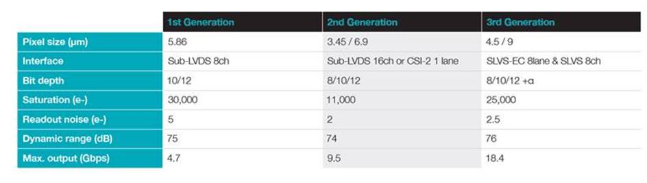
The base for this industrial success story is Sony’s Pregius technology. Pregius is a global shutter sensor – all pixels are exposed to light simultaneously – for active pixel-type CMOS image sensors that use Sony’s low-noise CCD structure, resulting in high picture quality and speed.
The third and latest Pregius generation provides functionalities like conversion gain switching, dual-trigger mode, self-trigger mode, and dual ADC to give higher industrial throughput and accuracy.
Sony’s Pregius technology is a main driver for the evolution from imaging applications used for classic machine vision to embedded vision systems within the production and inspection process of smart factories. Sony’s latest high-speed interface SLVS-EC supports higher frame rates from new sensors.
Future sensors will handle intelligence on-board
Although no official outlook was shown, branch experts believe Sony is working on future Pregius sensor generations, combining new sensor technologies and architectures for more resolution, higher frame rates and smaller packaging. This is especially the case for embedded vision applications where there are rumours of more MIPI interfaced sensors available within future developments, like the existing sensing devices IMX297/397 and the industrial 5-megapixel IMX335.
Today there are mainly front-illuminated CMOS global shutter sensors for high-speed inspection tasks. The Pregius line now includes resolutions ranging from VGA with IMX287/426 up to 32 megapixels with IMX342. Super high resolutions are available with Sony’s IMX461 and 411, focused on both airborne and space applications and wide-area surveillance, heritage and documentation tasks, as well as industrial and agriculture inspection. They reach 100 megapixels and 150 megapixels in medium-format type and come with back-illuminated CMOS pixels and high-speed SLVS-EC interface.
With its Starvis line of back-illuminated CMOS imagers, industrial rolling shutter sensors are still a key Sony focus area, mainly for security and surveillance applications not effected by movement artefacts. Sony’s rolling shutter portfolio has high sensitivity in the visible, as well as the near-infrared. Unlike the front-illuminated image sensors, the image is acquired through the back side where there are no obstacles such as wiring or circuits, so more light is collected on the photodiode, achieving high sensitivity with resolution up to 4K. Future Starvis developments will focus on small packages with low power consumption, which include low-noise miniaturisation for high definition images with greater signal-to-noise ratio, stacked pixel architectures optimised for AI monitoring, and region control features for data capacity reduction in security applications.
Sony’s future technology development
The representatives from Sony Japan said performance enhancement initiatives will include back-illuminated sensors for improved sensitivity, stacked architectures for miniaturisation and high functionality, copper-copper connection for better productivity and space savings, as well as pixel-parallel A/Ds for image distortion cancellation. Sony will also focus on function expansion, for example with lower power consumption for event-driven applications and region control features to reduce data capacity.
The first time of flight sensor demonstrations were shown at the Vision show last year in Stuttgart for distance information detection. Sony Polarsens imagers with four-direction on-chip polarisation for better distortion and scratch detection are also popular in the sensor market right now.
These innovations are based on Sony’s strengths in semiconductor design. The Framos Tech Days in San Francisco showed that Sony will continue its path as a sensor innovator helping to solve the pains of industrial end-customers.