Greg Blackman reports on CEA Leti's new image sensor, shown at Photonics West, which contains onboard processing and is able to image at 5,500 frames per second
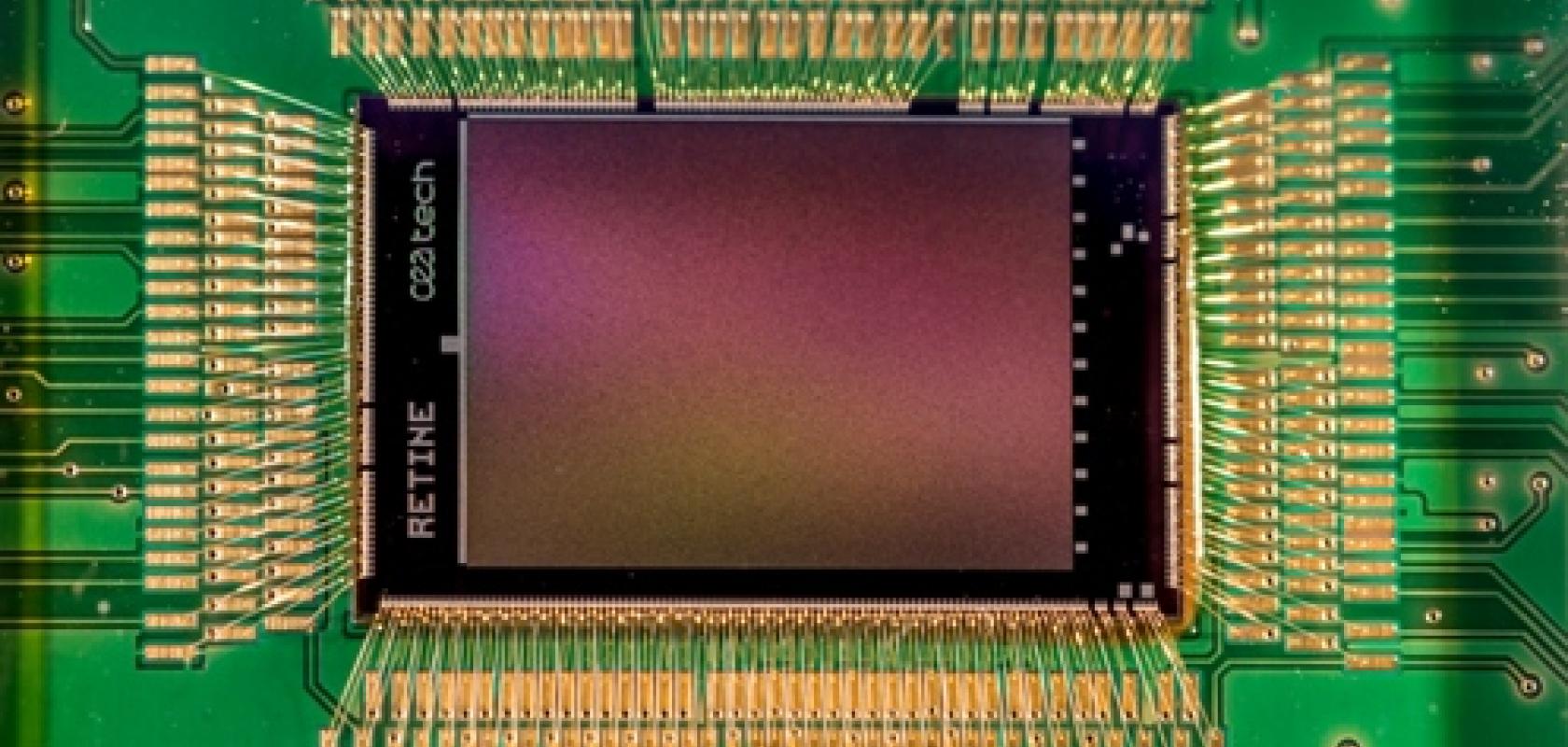
CEA Leti has presented a 3D stacked, backside illuminated, intelligent image sensor, able to run at 5,500 frames per second, during SPIE Photonics West in San Francisco.
The sensor’s architecture, which was designed together with CEA List, is much more energy efficient than conventional CMOS sensors, which have a serial output, because pixels send information directly to onboard processors in parallel.
The sensor is formed of photodiodes stacked on top of processing elements and memory. Each 16 x 16-pixel array – the photodiodes are backside illuminated giving higher sensitivity than frontside illumination – has its own processing element (PE), all connected in parallel. The data is sent over short connections to each PE, which means power consumption is kept to a minimum. In addition the processors run at low frequency, which decreases the voltage needed and improves energy efficiency.
The excellent efficiency of the sensor, its low latency, and its high frame rate – achieved thanks to the parallel access to processors – make the sensor suitable for monitoring fast-moving factory production lines, according to Marc Duranton at CEA, speaking to Imaging and Machine Vision Europe. Robot guidance or in augmented reality systems are two other potential applications for the sensor.
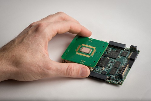
CEA Leti’s and List’s demonstrator chip has a resolution of 1,024 x 768 pixels with 192 processors of 16 PEs. The sensor and the processor dies are surfaced connected thanks to a Cu-Cu interconnect 3D stacking technique. The vision sensor has been integrated on an evaluation board with two FPGAs, USB and HDMI interfaces, and GPIOs.
As processors can run different code, the sensor is able to operate at a higher refresh rate in areas where there is lots happening in the scene, and lower refresh rates for other areas where there isn’t any movement. Scanning a background that’s not changing, for instance, doesn’t need to be imaged at 60fps – it generates a lot of redundant data.
The sensor, therefore, can be programmed to trigger and record important events according to what is happening in the scene, rather than analysing data continuously to locate the trigger. ‘There is a lot of communication and a lot of useless information [in a classical system] because you always have to scan data and to transfer it to an external processor,’ Duranton noted, ‘whereas, here the scanning and object detection is done in the sensor itself.’
Image analysis takes place directly inside the sensor onboard the 192 processors – the architecture is such that each set of 16 x 16 pixels could be processed independently. This opens up the potential for intelligence at ‘the edge’, rather than sending images for analysis to a separate machine. ‘You don’t need to have high bandwidth communication with the sensor, because the sensor is able to take the decision locally,’ Duranton explained. ‘[Avoiding] continuously sending video lowers bandwidth and power consumption.’
The architecture is also scalable, remarked Duranton, in the sense that the number of processors and the interconnect with the sensors increases in line with the number of pixels. ‘It’s not like a conventional sensor, where when you double the number of pixels, due to the serialisation, you need to double the frequency of the output data,’ he explained.
Copyright: S. Pajaniradja / CEA - 2018
Duranton said the sensor can scale to 4k or 8k pixel resolution. Compromises have to be made on the size of the system, in that imaging at high frames rates requires large photodiodes to capture a lot of electrons. At the same time, the processors take up space. However, even while running at 1,000fps the chip can execute about 1,000 instructions per processor. ‘We can do a lot even at a high frame rate,’ Duranton commented.
Duranton noted that some other image sensors are able to analyse data directly in the sensor, but the processing is dedicated to a particular algorithm such as white balance correction. ‘We really have a set of general-purpose processors,’ he said.
The next step, according to Duranton, is to develop the software library to improve functionality, as well as implementing neural networks for higher level recognition.
CEA Leti has also developed a curved image sensor – it was demonstrating this as well at Photonics West – that lowers the cost of optics in imaging systems. ‘We could also try to curve this [stacked sensor], so we could really have a sensor that’s like a human retina,’ Duranton said – ‘to have a low-cost optical system with low power and with the processing taking place directly in the sensor.
‘That’s more long term,’ he concluded. ‘We [CEA Leti] have the technology to curve the sensor and we have this stacked retina and, at some point, we would like to combine them.’
Top image: Copyright: S. Pajaniradja / CEA - 2018