Greg Blackman reports from SPIE Photonics West, where the first image sensors based on graphene-CMOS integration were on display
Broadband imaging based on graphene-CMOS integration has been demonstrated at this year’s SPIE Photonics West, which took place in San Francisco from 27 January to 1 February.
Frank Koppens from the Institute of Photonic Sciences (ICFO) in Barcelona, Spain presented several applications of graphene-CMOS integration, including the first monolithic integration of an electronic CMOS integrated circuit with graphene, operating as a broadband photodetector.
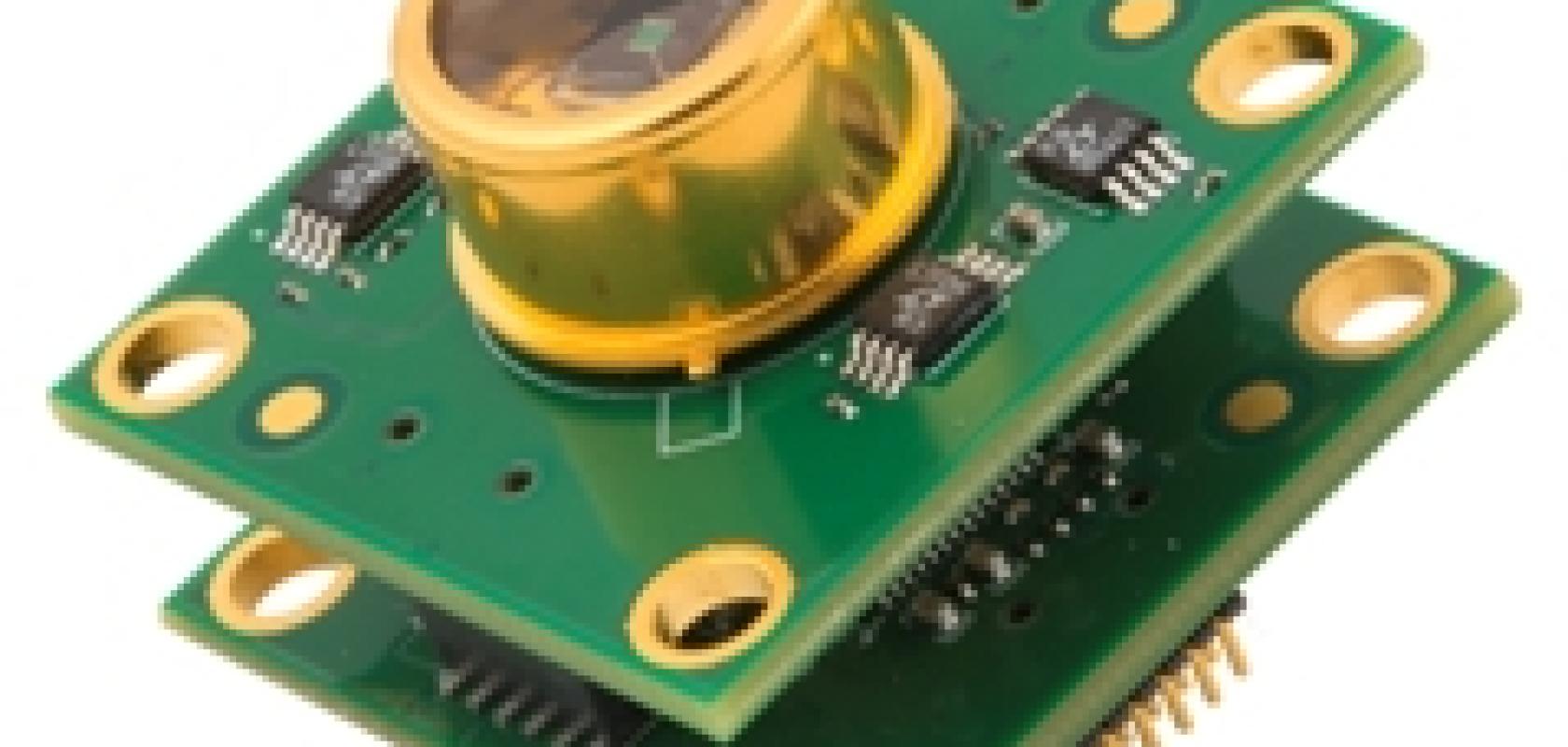
Meanwhile, Finnish company Emberion was exhibiting a new VIS-SWIR VGA (640 x 512 pixels) image sensor comprising a graphene photodetector array monolithically built onto a tailor-made CMOS chip.
Graphene is a one-atom thick layer of carbon. It has impressive material properties, one of which is its broadband absorption - detectors have been built for visible, infrared and even terahertz radiation. The EU is half way through its €1 billion Graphene Flagship programme, where the goal is to take the material out of the laboratory and make commercial products out of it.
Koppens commented during his presentation at Photonics West that a key advantage of graphene is the material can be combined with platforms like silicon CMOS.
‘You can take advantage of all the power that already exists in silicon CMOS technology and leverage the billions that have been invested in silicon CMOS and expand the functionality,’ he said.
Because graphene is a 2D material it can be transferred on top of silicon rather than having to grow the material. The layers are bound via van der Waals forces, which are still extremely strong, Koppens noted, because the material is only one atom thick.
Koppens’ team took a CMOS integrated circuit and replaced all the photosensors with graphene, layering the material on top of the silicon CMOS circuitry. The graphene was connected to the circuitry with vertical vias. The ICFO chip consists of 388 x 288 pixels.
Photodetectors have already been made with graphene that can sense across a broadband spectral range, but these are still based on one single pixel.
The graphene in the ICFO chip was sensitised with colloidal quantum dots to make it sensitive from 300nm to 2,000nm, covering UV, visible and infrared light. ‘At this point there is no technology that can do that on the market,’ Koppens said.
Infrared imagers can be costly pieces of equipment; the sensors are not based on silicon and can require cooling. A broadband imager operating into the infrared and made with existing silicon CMOS techniques could open up a range of uses from driverless cars to wearable electronics.
‘It's [graphene-CMOS integration] not better than silicon,’ Koppens said. ‘It’s almost impossible to compete with silicon CMOS [for visible light detection]. But compared to InGaAs, it’s comparable or better, but you also get the visible wavelength range for free.’
Sensitivity at each of the pixels on the ICFO chip is high. The team has demonstrated imaging through fog with the sensor, which is important for automotive and self-driving cars. The sensor has also been shown to be sensitive to starlight, meaning it can be used for night vision, which requires extremely high sensitivity between 1,500nm and 2,000nm.
Emberion’s VIS-SWIR VGA image sensor combines a monolithically integrated graphene detector array on a CMOS readout integrated circuit. It covers the spectral range from 400nm to 1,800nm; the pixel size is 20 x 20µm, the frame rate 100fps, and it has a dynamic range of 80dB. The sensor operates well at room temperature.
The company has also developed graphene-based bolometers for thermal imaging, which Dr Tapani Ryhänen, CEO of Emberion, noted had higher sensitivity than traditional bolometers. This means they give good performance without cooling, which could reduce the price of a thermal imaging system.
Emberion’s bolometers exploit heat-to-charge conversion using pyroelectric substrates coupled with charge detection using graphene field-effect transistors. They have a VGA array size, a spectral response of 3µm to 5µm and 7µm to 14µm, a video frame rate of 30Hz to 60Hz, and a noise equivalent temperature difference of 15mK to 30mK, uncooled.
Image: Emberion's graphene photodetector