The evolution of CMOS sensors has had an impact on most fields of imaging, not least in the life sciences. Scientific CMOS (sCMOS) sensors can now provide higher resolutions and higher signal-to-noise ratios than previously possible, challenging the high-performing but more expensive CCD technology. Taking advantage of these improvements, camera manufacturers this year have released products which offer a good balance between the two.
Both CCD and CMOS technologies have been developed to offer improved features for scientific applications such as fluorescence microscopy. The CCD sensors firstly evolved into the electron magnifying CCDs (EMCCDs) sensors to provide higher sensitivities and a better noise performance mainly at low light levels, whereas the sCMOS sensors have quite recently progressed to offer lower cost, higher pixel counts and faster speeds. With both technologies offering distinct advantages over the other, vendors tend to keep a variety of both cameras in their product portfolios, noted Flavio Giacobone, product manager of cameras for the Micro Imaging Solution Division at Olympus Europa.
Scientific CMOS technology has advanced considerably in recent years, however, and is beginning to rival the sensitivity and low noise levels of the EMCCD. Combined with the lower cost, faster frame rates and higher resolutions, sCMOS sensors are therefore becoming a popular choice for scientific researchers. ‘The emergence of sCMOS technology is a definite trend in high-end life science applications,’ said Giacobone. However, the sCMOS has not quite reached the performance of the EMCCD in some areas, as Giacobone reflected: ‘The noise and overall sensitivity of sCMOS sensors are not comparable with the EMCCD – although they have improved a lot, they have not yet approached that of the EMCCD.’
Sensitivity is important for scientific research, such as for a biologist observing cellular processes to understand their role in disease. In these types of application where live samples are used, light levels must be kept to a minimum to prevent any photo-damage to the cells. Particularly in fluorescence microscopy, the sensor may need to detect extremely small changes in light levels from samples stained with fluorescence probes.
In addition, the camera must be capable of capturing fast-moving live processes. This is technically challenging as fast events require short exposure times, but this in turn means fewer photons of light can be captured – hence cameras suitable for scientific research combine high sensitivity with careful electronic design to minimise noise sources that could otherwise drown out the sample’s signal.
In September, Hamamatsu launched a new EMCCD camera, the ImagEM X2-1K, which can deliver up to 314 images per second. It was designed for a range of applications, from genetics studies (capturing luminescence) through to the detection of fast events such as neuronal activity through calcium reporters. It is capable of imaging in ultra-low light conditions of fewer than 10 photons per pixel between the sample and background. ‘The collected photons are converted into photoelectrons and are multiplied through impact ionisation. This analogue signal is then digitised and displayed as an image by the PC,’ explained Dr Ruediger Bader, sales engineer at Hamamatsu Photonics UK.
Affordable high performance
sCMOS technology is fast approaching sensitivity levels of EMCCD sensors, according to Giacobone: ‘For extremely low light level imaging, for example, EMCCD is still the go-to technology, but the rapidly evolving sCMOS is challenging this. Improving year-on-year, we can expect them to reach a similar level of performance in about three years.’
In applications with more standard requirements CMOS sensors are more cost-effective than the CCD, so camera manufacturers are increasingly incorporating the former into cameras, and employing correction technologies to boost the sensitivity and reduce noise. This approach retains the image quality of traditional CCD cameras while providing substantial cost savings: ‘What is happening is that you take a sensor that is cheaper to produce, and build upon it using clever technologies, creating images suitable for scientific analysis,’ Giacobone pointed out. ‘This is part of the overall trend, where software is used to enhance cheaper sensors, in order to generate a higher quality image.’
For example, the latest CMOS camera from Olympus, which was released in November, fits in the ‘affordable high performance’ category, combining the cost benefits and faster frame rates of CMOS with more sensitive and noiseless images, improving image quality at lower cost.
To increase sensitivity as well as achieve speeds up to 32 frames per second, the SC50 contains a light guide feature which focuses the photons directly onto the most sensitive part of the sensor, instead of them being scattered within the chip material. In addition, the Smart Image Averaging software addresses noise by taking a series of pictures and isolating the noise from the signal, using a smart algorithm to detect sample movement and temporarily halt the averaging process, avoiding artefacts while moving and focusing on the sample.
Large chips, large field-of-view
Another reason why sCMOS sensors are in demand in the scientific sector is that they can capture a large field of view at high resolutions. CMOS chips are larger and have higher pixel counts of between four and six megapixels, as opposed to EMCCD sensors that have less than one megapixel resolution.
Having a large field-of-view and the capability to zoom in retrospectively is of particular interest to scientists working in fluorescence microscopy.
In contrast to the common misunderstanding that higher magnifications require higher camera resolution, higher resolution is, in fact, only effective when working at low magnifications. Giacobone added, ‘when using a 60X or 100X oil objective, for example, a one-megapixel camera will normally be sufficient; a higher pixel count will just increase data volume without providing any extra information. However, when using lower magnifications, higher pixel counts are required to capture more detail, allowing the user to zoom in afterwards.’ For this reason, as Giacobone explained: ‘We have an increasing number of customers who no longer use 60X or 100X objectives in fluorescence imaging, instead wanting to use maybe a 20X or a 10X objective.’ When wanting to correctly capture all of the optical resolution, the required megapixel count rapidly increases as the magnification decreases. Simply put, if you want to capture a bigger area containing a lot of detail, you need a higher number of pixels, and finer pixels, to capture those details.
Having a larger field-of-view with a higher resolution not only provides the scientist with more information, but increases the speed of imaging. One method used to create an image of a larger sample area is to scan smaller areas of the sample, and then stitch the images together to form a large picture which the user can later zoom in on. Giacobone explained: ‘Think of Google maps − it is basically a collection of small images that you can pan around and zoom in on.’ By having a larger sensor, at each scanning step the camera can capture a larger section of the sample, meaning that fewer scanning steps are involved, and the sample can be scanned more quickly.
‘The industry is shifting towards bigger chip sizes,’ Giacobone added. ‘The trend is towards having a one inch sensor or more in every type of camera, either colour or monochrome. Interestingly, the evolution in this area mimics what is happening in the consumer market.’
USB 3.0
With larger sensor sizes and higher resolutions pushing data rates up, the USB 3.0 interface is being used more widely for its ease of use and high data transfer speeds. USB 3.0 overcomes many of the limitations of Camera Link, which include the need for a capture card or a frame grabber inside of the PC, or having to have bulky cabling. ‘[Camera Link] is very difficult to work with − nobody wants to use desktops anymore,’ said John Phillips, product manager at Pleora. ‘We can see this if we go to any computing market study; people are buying laptops or tablets, there is not a lot of growth in buying desktops.’
To take advantage of the USB 3.0 interface, Pleora has developed a device − the iPort CL-U3 − which can convert Camera Link Base or Medium to USB 3.0 so it can be plugged into any USB port. It was designed to improve the ease-of-use for existing owners of Camera Link cameras, and to provide more flexibility to customers who may want to purchase a Camera Link camera but do not want a frame grabber or bulky cables. ‘A lot of the cameras that are used in the life sciences and microscopy market still to this day are Camera Link, either because the cameras are legacy cameras which the user has bought a few years ago and they still want to keep, or because the sensors they want to use are only available inside of cameras that have Camera Link outputs,’ Phillips noted. ‘Both of those scenarios we see all of the time.’
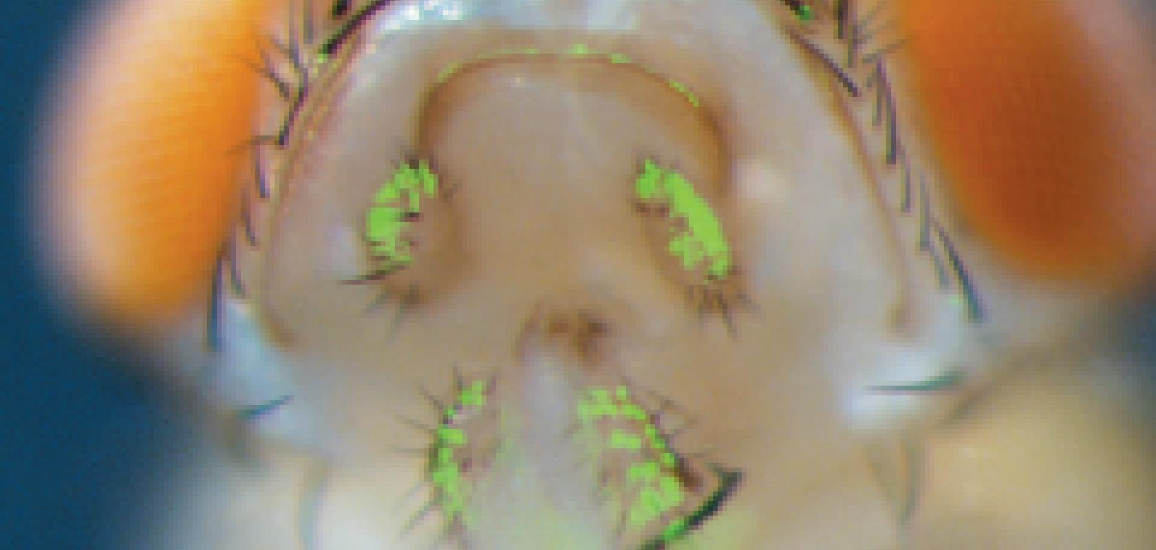
Imaging different dyes simultaneously
Another requirement for scientists working in fluorescence microscopy is to carry out both colour documentation and fluorescent detection simultaneously. This is needed when, for example, histological stains and fluorescent dyes are used on the same sample, or, when a live subject has been altered to produce fluorescence. ‘You might have a living organism where the genes have been triggered to express green fluorescence protein. So, you not only need to image its real life colours but you also want to see where these fluorescence expressing genes are located,’ explained Olympus’ Giacobone.
These types of research scenarios require two cameras on the microscope; a colour one as well as a camera that is sensitive to fluorescence. Traditionally, to acquire the final mixed image, a mechanical switch is used to change the optical path between both cameras, and the fluorescence image is subsequently overlaid over the colour one. However, the process can create some challenges, according to Giacobone: ‘There may be issues because the two cameras may not be aligned perfectly, so you may have to align the two images manually afterwards and this may be time-consuming in some cases,’ he said. ‘And then there is the inconvenience of manually switching this optical path, an operation which may need to be repeated hundreds of times for a complete study.’
Overcoming these challenges, Olympus’ DP80 camera combines a colour and a monochrome sensor, with control software to switch between the sensors automatically. The sensors are pre-aligned, which means images are automatically and precisely overlaid, without user intervention. ‘Inside the DP80, there is a highly precise mechanical switch, making sure that the correct chip is in the optical path, and that the alignment is maintained over time,’ noted Giacobone. ‘It is automated, very precise, quick, and guarantees effortlessly mixed fluorescence and brightfield images.’
Multi-wavelength imaging is another technique for detecting two different dyes on a sample. This is particularly useful for fluorescence microscopy, as the vast majority of applications in this field involve the use of more than one fluorescent probes. ‘[Using two fluorescent dyes] is for example important for co-localisation studies,’ noted Hamamatsu’s Bader.
For these types of study, cameras containing image splitting optics are used. The W-View Gemini from Hamamatsu contains a dichroic mirror and two fluorescence filters, which enables the acquisition of dual colour fluorescence, Bader added. ‘It has also the capability to correct for chromatic aberration very easily.’