Researchers from Imec have developed a new imager implementing CCD TDI pixels together with advanced CMOS drivers and readout in one single chip. This CCD-in-CMOS technology is compatible with backside illumination for enhanced sensitivity, and multispectral filters can be added for increased imaging performance.
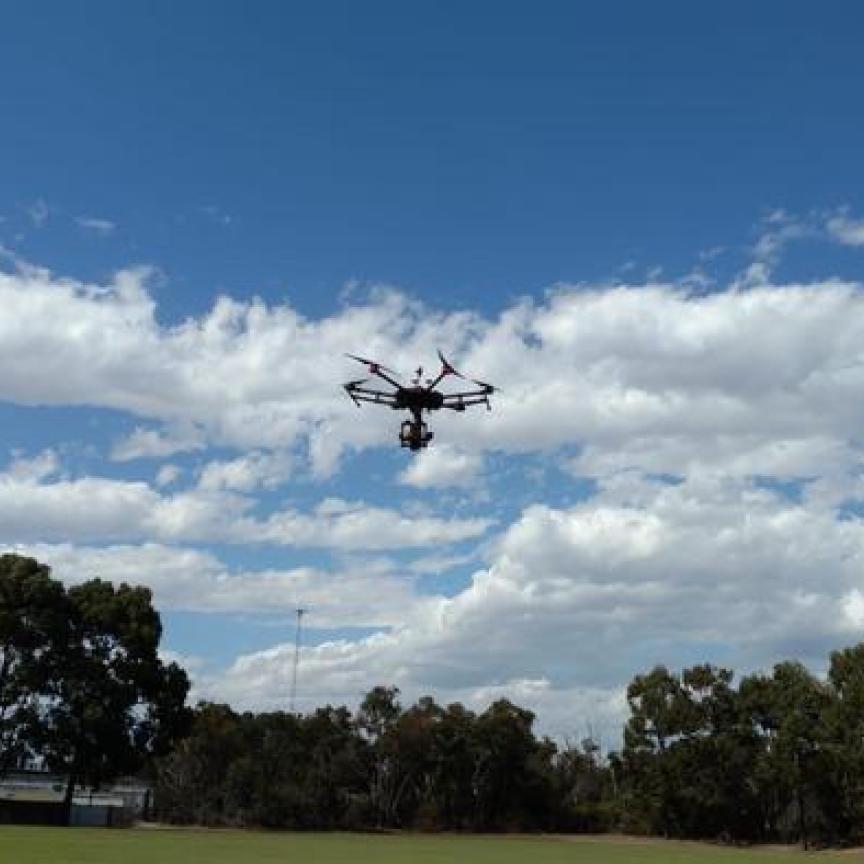
The prototype TDI sensors use a format with 4,096 columns and 256 stages per CCD array, or band. A version with one CCD TDI array is available, as well as a seven-band version, meaning seven spectral filters can be added. With this highly sensitive and high-speed imaging solution, Imec is targeting high-end applications such as remote sensing, life sciences and machine vision.
Time delay and integration (TDI) imaging is a preferred line scanning technique used in applications such as industrial inspection and earth observation. The technology of choice for collecting and transferring the pixel signal is charge coupled device (CCD) sensors.
Using CMOS imagers for TDI is also an option – the advantage being CMOS’s high degree of electronic circuit integration, as fast readout electronics can be integrated on the imager chip itself. The disadvantage – as compared to CCDs – is an increased noise, and a need for large memory and fast data processing.
Traditionally, a CCD system requires a board with multiple chips, including the CCD, drivers and readout chip. Imec has been developing a new solution that combines CCD pixels and CMOS readout in one technology, enabling a single imager chip with both CCD and CMOS functionality. This solution combines the best of two worlds: the noiseless collection and transfer in charge domain of CCDs, and the system integration potential and the low power and fast readout that only CMOS can deliver. Contrary to traditional, CCD-based TDI imagers that read out pixels per column and multiplex the data to one off-chip analogue-to-digital convertor (ADC), the new imager uses column-based ADCs. In this configuration, one ADC is used per CCD column, and the different columns are readout in parallel. This results in a high readout rate with low power consumption.
While CCD imagers are typically manufactured on 150mm wafers using dedicated processes, Imec has developed a CCD process module inside its 130nm CMOS process flow on 200mm wafers. This results in a more cost-effective manufacturing flow. The process is also compatible with other wafer-level post-processing techniques such as backside illumination and spectral filter integration. The use of backside illumination gives enhanced sensitivity, and the addition of multispectral filters results in improved imaging performance.
From earth observation satellites to cell sorters
One of the first markets that made use of TDI-based cameras is earth observation from space, using large satellites. By combining CCD-based TDI technology with advanced CMOS readout electronics, the system complexity and size is reduced, making the technology suitable for implementation into small satellites. Adding multispectral filters on top of the CCD-in-CMOS TDI sensor makes it particularly interesting for environmental monitoring, precision agriculture, and disaster detection and monitoring.
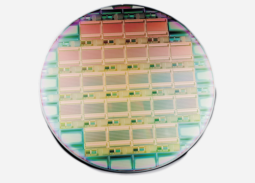
200nm wafer with CCD-in-CMOS imager
A second market is industrial machine vision where, typically, products are moving linearly on a conveyor belt. Examples are flat panel inspection, semiconductor front-end inspection, printed circuit board inspection, and glass inspection. For these applications, the high scanning speed of the imager is a key characteristic.
An emerging application field is life sciences, where massive amounts of cells or tissue need to be scanned at a very high speed. Potential applications include DNA sequencing, or cell cytometry. Another potential application is slide imaging for diagnostic purposes in pathology.