
Imec is working to industrialise thin-film photodetector stacks on CMOS in order to fabricate low-cost infrared image sensors, as the Belgian institute’s Dr Paweł Malinowski explains
Image sensors have come a long way from replacing film cameras by CCDs and becoming a commodity by switching to CMOS. Most of us own at least five or ten of them, even if we are not fully aware of it – a smartphone can have several sensors; then there are those in webcams, cars, toys, doorbells and so on. Mass manufacturing on wafer level and standard design kits bring the production cost into the range of single euros per integrated camera component.
At the same time, one of the global trends in imaging is a switch from photography to sensing, where a picture is either not enough or not necessary. In an autonomous car, for example, images of the road are not needed; the car needs information about whether there is an obstacle in the road and what type of obstacle it is.
Next to that, another trend is a shift into the near infrared range. Operating at 850nm or 940nm wavelengths, which can still be detected by a silicon photodiode, opens up applications such as structured light depth sensing. Going further out to 1,450nm takes advantage of low background radiation in terrestrial applications (water absorption window), while operating at 1,550nm means the imager can see through fog and clouds (water transmission window) and use the night glow for low-light imaging, such as in surveillance applications. The fundamental issue here is that CMOS image sensors are not sensitive to radiation above approximately 1µm because of the energy bandgap of silicon. This is why epitaxially grown III-V or II-VI materials are used as the absorbing layer in the photodiode. Low throughput of the base material growth and high integration complexity unfortunately prevent mass deployment of infrared imagers made from III-V or II-VI materials.
The alternative approach – followed by several companies – is to use a combination of a silicon-based readout chip and an external photodiode replacing the silicon one. This can be based on thin-film stacks with a photoactive layer sensitive in the infrared. Such a photodiode stack can be deposited directly on full wafers for scalable production and thus very low cost. This also enables small pixel pitch, limited only by the readout technology node, while extending the sensitivity range, even to 2µm, depending on the active material selection. The challenge is to develop an efficient pixel stack, composed of the active material and supporting materials, such as transport layers, alongside an integration scheme to connect it with the silicon readout.
At Imec, we tackle the full process flow, including designing readout pixels and circuitry, and developing back-end-of-line interconnects that are processed on readout wafers in Imec’s 200mm fab. In parallel, we are working on a portfolio of thin-film pixel stacks tuned for a variety of applications. One example is polymer photodiodes with broadband absorption from 300nm to 1,100nm. Another is a family of colloidal quantum dot photodiodes with visible absorption and an additional sensitivity peak, related to the quantum confinement, which can be tuned for sensitivity between 900nm and 2,000nm by changing the quantum dot size. For prototyping, Imec integrates imager chips on die level and, in parallel, develops full 8-inch and 12-inch wafer process flows to enable mass manufacturability.
Our first prototypes confirm the feasibility of imaging wavelengths above 1µm with small pixel pitch and in a very compact, low-cost form factor camera. Looking further along the development roadmap, there are three potential approaches for thin-film infrared image sensors.
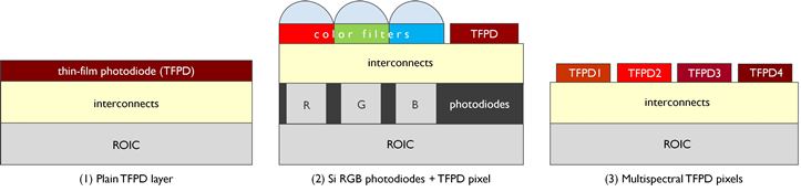
The first implementation is the simplest, as it only assumes a plain layer of the thin-film photodetector stack. In this case, not taking into account any filters, all pixels have the same absorption spectrum. This is defined by the active material, for example a 5.5nm PbS quantum dot sensitive in the visible with an absorption peak at 1,450nm. One application could be wavelength extension of a face scan sensor in front-facing smartphone cameras. Going to 1,450nm means better background rejection, important for imaging in bright sunlight, for example. Furthermore, such a solution could be considered for operation in the eye-safe region, allowing higher power light sources to be used in applications like augmented reality for scanning larger areas.
The second implementation takes advantage of pixelation of the thin-film stack, which is one of the strong areas of expertise at Imec. Here, an infrared subpixel could be added next to the red, green and blue photodiodes, realised as a silicon pinned photodiode. This would add an additional wavelength band, or layer of information, to visible cameras. A separate sensor for structured light would not be required using this solution, reducing both the system footprint and power consumption. One might envision very low-cost cameras with depth sensing capabilities.
The third implementation builds further on the pixelated stack, this time placing stacks with different active materials side by side. Such a configuration would enable pixel-level multispectral sensors in the near infrared and shortwave infrared ranges, keeping a very compact form factor and a price point still in the realm of silicon image sensors. Having 1,450nm and 1,550nm pixels next to each other could offer both compatibility with long-range illuminators and passive visibility at low-light and in difficult atmospheric conditions. Implementing pixels for characteristic wavelength bands would enable the camera to distinguish between materials with different spectral footprints, which is especially useful for material sorting applications.
In summary, thin-film photodetector stacks can enable low-cost, high-resolution infrared image sensors. Imec is developing full wafer process flow to industrialise this approach. In parallel, the organisation is optimising the pixel stacks for particular applications. The first prototype chips show not only successful image acquisition, but also video rate capture.
We are currently looking at the achievable operating speeds for different material stacks. Also, stability at elevated temperatures needs to be tested to verify this concept’s suitability for automotive applications. The exciting prospect is that the choice of pixel stack is limited only by the creativity of chemists and material scientists. This means that, with a full wafer integration process in place, we envision a quasi-unlimited family of pixel stacks fine-tuned for acquisition of very specific information. Thin films, even though only hundreds of nanometres thick, will enable further growth of the imaging industry well beyond photography, especially for wavelengths above 1µm.
Dr Paweł Malinowski is program manager for user interfaces and imagers within the thin film electronics group at Imec.