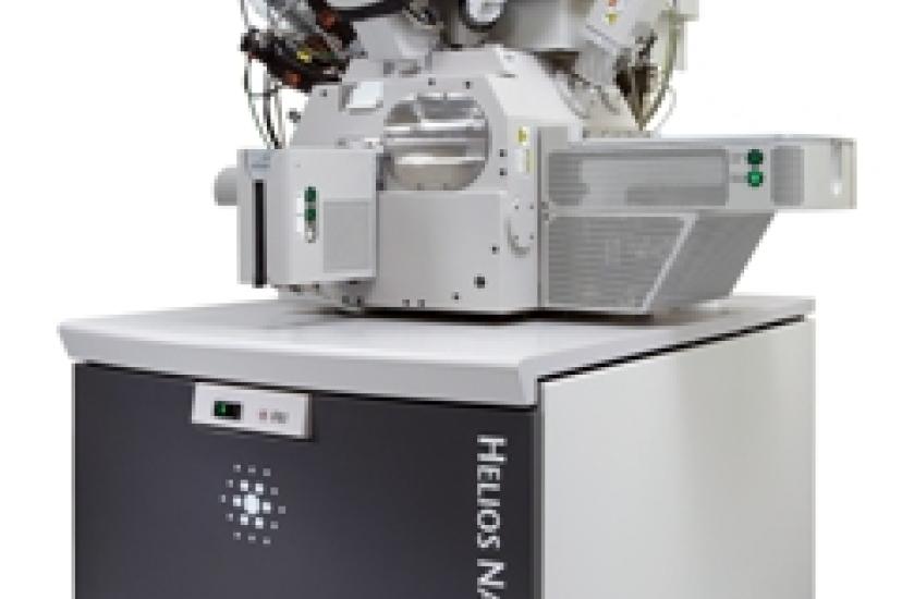
Scios and Helios NanoLab 660 DualBeam systems
FEI has introduced two DualBeam focused ion beam (FIB), scanning electron microscopy (SEM) systems, ideal for materials research applications
FEI has released a suite of solutions for correlative light and electron microscopy
FEI has released the 
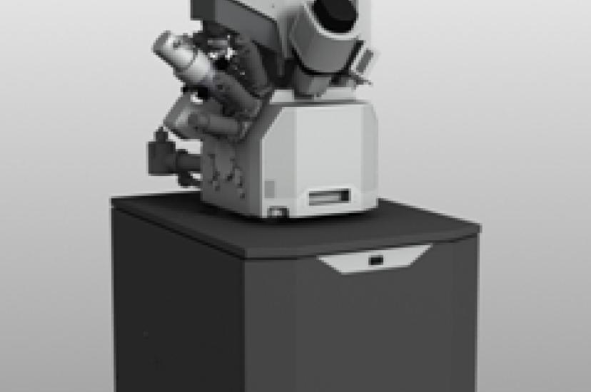
Helios NanoLab 450 F1 DualBeam electron microscope, designed to provide semiconductor manufacturers with faster, better images of advanced device architectures
Instrumentation company FEI has added a UniColore (UC) monochromated electron source to its Versa 3D DualBeam system
Susan Fourtané on the increasing demands being placed on web inspection solutions to achieve zero-defect manufacturing
Facing new pressures and demands, logistics operations are calling for adaptable machine vision solutions to drive efficiency, discovers Benjamin Skuse
Luca Verre, Co-founder and CEO of Prophesee, as well as a Photonics100 honoree, highlights how event-based vision is set to revolutionise mobile photography
Hunting defects in the soon-to-be trillion-dollar semiconductor industry is big business. Anita Chandran explores the latest wafer inspection technology