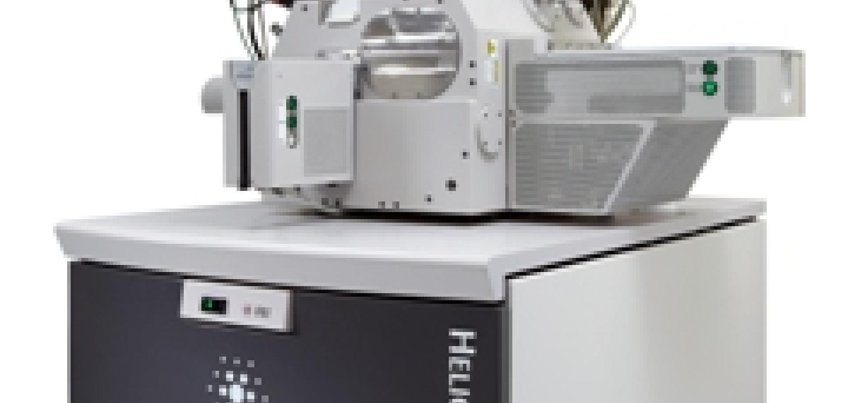
FEI has released the Helios NanoLab 450 F1 DualBeam electron microscope, designed to provide semiconductor manufacturers with faster, better images of advanced device architectures. A new STEM (scanning transmission electron microscope) detector delivers improved contrast between materials, and the new flip stage and rotating nano-manipulator support advanced preparation techniques for complex device architectures, such as finFETs and 3D memory structures.
The Helios NanoLab 450 F1 is the most recent addition to FEI’s line of DualBeam systems. It combines high resolution scanning electron microscope (SEM) and focused ion beam (FIB) for high quality imaging and fast, precise milling and deposition, and adds capabilities specifically designed for semiconductor failure analysis applications.
The new STEM detector delivers higher resolution and better material contrast. The FlipStage 3 quickly flips the sample between thinning and STEM viewing positions and a new rotation axis permits viewing from either side of the section. The EasyLift nano-manipulator provides precise motorised sample manipulation, including rotation, to support automated lift-out and advanced preparation procedures, such as inverted thinning. The MultiChem gas injector system provides excellent flexibility in gas-assisted milling and deposition, while also cutting maintenance costs with pre-filled crucibles.