ANDANTA’s InGaAs-VGA “BADGER” image sensor family will soon be complemented by a VIS- InGaAs sensor, which is also sensitive in the visible spectral range. The sensor FPA640x512_P15- C-VIS (BADGER-C-VIS) can have a quantum efficiency of up to > 80% (min. > 70%) in the infrared (900nm – 1700nm) and up to > 50% (min > 30%) in the visible spectral range (down to 600nm).
The BADGER InGaAs-VGA sensors have already attracted a lot of attention from near-infrared camera manufacturers right after their market launch. Thanks to economies of scale, the prices of the sensors have now become even more attractive.
The VGA-BADGER sensors come with a reduced pixel size of 15 μm (formerly 25 μm), reducing the total active sensor area to just 9.6 x 7.68 mm, identical to the low-resolution, QVGA sensors FPA320x256. This eases the integration of the VGA-sensor for all existing users of the ANDANTA QVGA sensors. The use of 8 outputs with 18 MHz pixel rate provides a read out rate of nominal ≥ 300 fps at full image and faster (users also report of possible 600 fps through overclocking). Moreover ≥ 30,000 fps are possible for the smallest subwindow of 32 x 4 pixels (with 8 outputs).
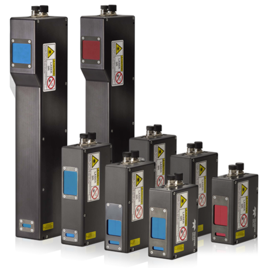
The sensor is available in uncooled, 1-stage and 2-stage thermoelectrically cooled versions. The uncooled FPA640x512_P15-C (BADGER-C) uses a simple, hermetic 64pin ceramic LCC package with a size of only 18 mm x 18 mm x 2 mm and a sensor weight of just 1.7 g, thus allowing a very compact and lightweight camera design with low power consumption of max. 200 mW as there is no cooler to drive.
The same InGaAs sensor chip is also available in a Kovar package with a 1-stage (FPA640x512_P15-TE1 = BADGER-T1) or a 2-stage (FPA640x512_P15-TE2 = BADGER-T2) thermoelectric cooler. A hermetic 28-pin metal shrink dual inline package (SDIP) is used for this purpose, with a pin pitch of 1.78 mm, a size of just 36.1 mm x 25.4 mm x 7.3 mm (without pins) and a sensor weight of just 19.5 g. In the 2-stage cooled sensor, the chip is placed in the sensor package 1.1 mm higher than in the 1-stage cooled sensor with the same sensor package, since the 2-stage cooler requires more space.
To better adapt the sensor to an existing temperature control, the user can now choose between a cooler version with high cooler voltage and one with high cooler current (different cooler resistances). The user can now also select 2 different options of the integrated readout circuit, which differ from each other for the 3 possible sensor gain settings mainly with regard to the conversion efficiency in μV / e- and the charge carrier capacity in e-.
The 2-stage cooled version is also available with extended spectral range from 1.2 μm to 2.2 μm, (FPA 640x512_P15-2.2-TE2 = BADGER-2.2-T2).
The peak quantum efficiency of the 2.2 μm sensor can be up to > 80%. According to the data sheet ≥ 60% are guaranteed broadband in the spectral range from 1.4 μm to 2.1 μm at -40 ° C chip temperature, adjustable by the integrated 2-stage Peltier cooler.
The 2-stage cooling proves to be very advantageous with the extended 2.2 μm InGaAs image sensors, because the dark noise and the signal non-uniformity over the pixels are higher than with the 1.7 μm versions, and can be significantly reduced by the more powerful cooling. The crosshatch signal distribution across the pixels, which is typical for 2.2 μm sensors, is effectively reduced by the 2-stage cooling as well.
All these features give the user a high degree of flexibility in adapting the image sensor or the camera to the target application.
Upon request ANDANTA can recommend suitable sockets to hold the sensors.