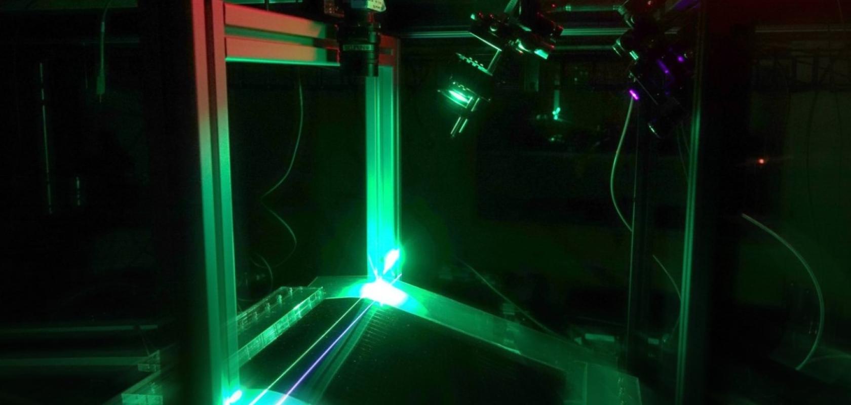
Researchers at the Fraunhofer Institute for Material and Beam Technology IWS have developed a solution that uses artificial intelligence (AI) and optical measurement technology to identify defects in real-time.
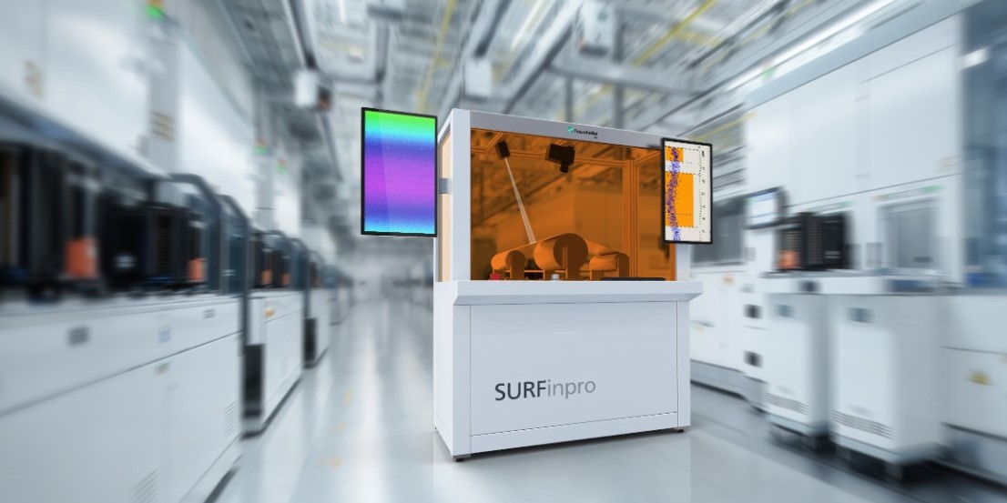
Known as SURFinpro, the solution detects, classifies and visualises defects, artefacts, and texture changes, and evaluates them using AI.
By quickly capturing the 3D information of surfaces in high resolution, the process could help to speed up production processes, the researchers say.
Dr Christopher Taudt, group manager for surface metrology at the Fraunhofer Application Center for Optical Metrology and Surface Technologies AZOM, (part of Fraunhofer IWS) said: “The system does not just detect defects — it classifies them at the same time and immediately establishes a wider context. Our customers receive information about the type of defect, along with many other parameters like the defect’s density, geometric dimensions and frequency.”
For over a year, the system has been used to analyse a roll-to-roll process with substrate widths of 70cm. Now, the SURFinpro team is training it in production by using a defect catalogue. Reported defects are fed into a neural network to enhance the system’s detection accuracy. The researchers then use the measurement information to identify new or modified defects. In this way, they plan to develop better neural networks that require less data.
Thanks to a sophisticated modularisation approach using efficient components, the researchers say, SURFinpro has a wide variety of potential deployments and is easy to adapt
The scientists say that thanks to a sophisticated modularisation approach, SURFinpro can adapt to a variety of tasks. They have their sights set on applications such as continuous fibre-composite manufacturing processes and the production of flexible semiconductor materials.
“Many of the technologies that we use in our system have been developed as standalone components in a way that they can also be implemented effectively in various other contexts and projects,” said Taudt. “Here, our partners are not only interested in avoiding near-surface defects – they also want the technology to be able to identify and assess components in multiple dimensions.”
The team is also working on increasing the speed of the system, especially for use with fibre-reinforced plastics and in textile processing – tasks that require very short cycle times.
Taudt explains: “Increasing speed is an important issue and we have the expertise to meet these requirements. Our solution uses machine learning and AI technologies firstly for the actual analysis, but also to accelerate the assessment steps. An effective measurement analysis process consists of a manageable number of individual steps that filter and reduce data. We are continuously developing new technologies in this area in order to make this process even faster and to extract the same amount of information from less data, for example.”
The team will present their system at the Laser World of Photonics in Munich later this month, at booth 441 in hall A3.
Images: Fraunhofer IWS