Heightened quality control measures might be low on the priority list of solar cell manufacturers at the moment, struggling as they are to make a profit with government cutbacks in the photovoltaic sector taking their toll, but work continues on improving QC techniques nonetheless. Luminescence inspection is deemed particularly important for crystalline solar cell production, as it uncovers defects in the silicon and gives a direct measure of the efficiency of the wafer, cell or module.
Dr Bram Hoex, director of the silicon PV cluster at the Solar Energy Research Institute of Singapore (SERIS) goes so far as to regard luminescence imaging as ‘the biggest innovation in solar cell and module analysis of the last decade’.
‘It’s a massive leap forward in terms of analysis and it’s so quick,’ he says. ‘It should be used in quality control checks, because so many performance-limiting defects can be picked up with this characterisation technique. Some of these defects cannot be detected by the current standard testing sequence.’
Luminescence imaging assesses non-uniformities in the silicon wafer or solar cell by exciting the semiconductor to emit light, either by driving a current through the cell, known as electroluminescence (EL), or bombarding the silicon with photons, called photoluminescence (PL). Exciting silicon causes it to act like an inefficient LED, the light produced from which gives diagnostic information on the material’s efficiency at generating electricity.
‘EL is already widely used in the solar industry,’ states Hoex. ‘Most solar manufacturers employ EL off-line currently, but inline EL will become more prevalent in the future.’ EL is simple to implement but it requires electrical contacts to be made and a current to be passed through the cell, so it can’t be used to test raw silicon.
PL imaging is a little more complicated because the luminescence signals tend to be relatively small. It involves a high-power light source, typically a laser, and the ability to filter out undesired wavelengths. However, the technique is non-contact, so it can be implemented right at the beginning of the process to test the unrefined silicon.
PL is a less mature technology, but there are some companies selling inline equipment, notably BT Imaging, based in Surry Hills, NSW, Australia, which provides equipment for sub-second PL imaging of silicon wafers. Isra Vision (Darmstadt, Germany) also supplies both inline EL and PL inspection systems as part of its Solarscan product range. The Solarscan-PL system incorporates homogenised illumination to provide an inspection field of up to 170 x 170mm. Both Isra Vision’s and BT Imaging’s systems offer inspection speeds of 3,600 wafers or cells per hour (one wafer per second), exceeding current production speeds, which, according to Hoex, run at around 2,000 wafers per hour.
Hoex feels the first wide-scale industrial application of PL imaging will be applied in the sorting of raw silicon wafers. ‘After sawing of the wafers, their electronic quality can be assessed before they are processed into a solar cell,’ he says. The test means wafers can be sorted according to quality and any defective ones removed. Production lines can therefore be optimised for processing a more specific range of raw wafer quality.
The type of luminescence typically employed is bandgap luminescence, which is measured around the bandgap of silicon at 1.1eV, emitting at around 1,100nm. Silicon CCD cameras are the usual choice for measuring emissions, as they are still sensitive at this infrared wavelength and are significantly cheaper than InGaAs cameras.
There have been, however, some improvements in InGaAs cameras that make them more suitable for luminescence imaging. Belgian company Xenics provides line scan InGaAs cameras used for PL and EL inspection. Raf Vandersmissen, CEO of sInfraRed, a Xenics subsidiary based in Singapore, comments that line scan gives the advantage of relatively low cost compared to area scan InGaAs versions, combined with high resolution. Xenics’ newest line scan InGaAs camera offers 1,024 pixel resolution and the company also plans to release a 2,048 pixel version later in the year. ‘We see a lot of interest in the infrared line scan business in Asia,’ Vandersmissen says.
‘In the past, [photovoltaic] customers were comparing Megapixel cooled CCD arrays with an InGaAs 2D array with a 320 x 256 pixel resolution. We had a big problem with infrared cameras in that the price was still higher than CCD cameras and the resolution was a lot lower,’ Vandersmissen states. ‘Now, with a line scan system, we are roughly at the same price level and the resolution is also about the same as CCD cameras.’
The advantage with InGaAs cameras is that they have a better efficiency in the 1,100-1,200nm wavelength band, so they can operate at much shorter exposure times. Therefore, for inline systems, InGaAs will be able to inspect at much higher speeds.
‘The problem why InGaAs never broke through completely in solar cell production is that the most common defects are still visible with a silicon CCD camera,’ Vandersmissen summarises.
Hoex feels that the main performance-limiting defects that can be identified by bandgap luminescence would already be a step up from the current QC checks in terms of real-time monitoring on production lines. ‘Sorting wafers with PL would be a great improvement especially for the latest generation of silicon crystalline material,’ he says, referring to cast monocrystalline (cast-mono) silicon, a relatively new material which combines the higher efficiency associated with monocrystalline silicon with the lower costs of the polycrystalline version. This material can look good on the surface, but under closer inspection with PL imaging, a lot of performance-limiting defects emerge. It just takes one PL image, Hoex says, with no need for further sophisticated analysis. ‘There will be a wide array of yield variation with cast-mono silicon wafers. This could result in a big push for more inline metrology at the wafer selection stage,’ he comments.
However, Hoex concedes that the use of this inspection technology will ultimately come down to cost. He says: ‘PL has tremendous potential, but the cost-benefit analysis has to be positive in the very short term in the PV industry. This is still a difficult business case for equipment suppliers for metrology.’
Extended defects
Bandgap luminescence will give a good indication of the efficiency of the solar cell, but there are other extended defects emitting at longer wavelengths which do require cooled InGaAs cameras to detect. Investigation into these types of defects is generally the realm of R&D, as they require more specialised equipment to study and are less well understood. Xenics sells high-end InGaAs cameras for these scientific photovoltaic applications. Vandersmissen comments: ‘This isn’t a market where you can sell hundreds of cameras a year, but it could still be a market for 20-50 cameras per year.’

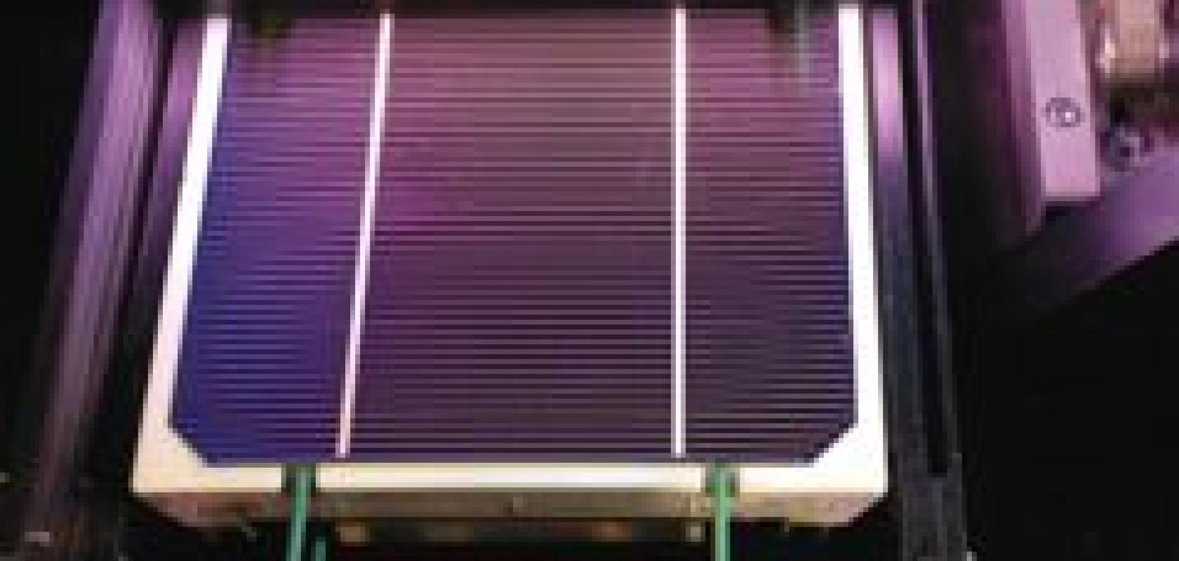
Electroluminescence image of a solar cell; the dark areas show broken connections. Credit: Solar Energy Research Institute of Singapore
SERIS is investigating extended defects – crystal imperfections in the silicon lattice – that emit at around 1,500nm. The researchers have shown that the photons emitted at around 1,500nm can have a preferential polarisation state. ‘By using standard polarisers, we’ve shown that the polarisation state of the photon carries some information from where it was emitted,’ explains Hoex. ‘We postulate that this could potentially be a way to get more information about the defect and, if it can be applied, a way to determine the origin of defects over a whole silicon wafer.’ Hoex and his team are using InGaAs cameras for these studies, along with an IR polarisation filter.
Potentially this imaging technique at 1,500nm could be used to inspect raw silicon wafers and even silicon ingots. It would help in selecting wafers and determining which ones could be processed to mitigate defects (dislocations in the silicon lattice can be altered by processing at certain temperatures). ‘The advantage of this technique is that it is really looking at defect luminescence,’ Hoex states. ‘Dark areas in EL images, for example, can have various root causes, whereas this technique identifies the cause of the defect, to discriminate between different variations of flaws in the wafer.’ He suggests that among the first applications of this technique might be to serve as feedback to crystal growers for optimising the furnace recipes.
SERIS is also looking at quantifying material properties of silicon thin film solar cells using luminescence imaging, mainly with EL imaging as thin film cells are less efficient as an LED and therefore require higher inputs of energy to get a measurable signal.
Value-added production
Luminescence isn’t the only inspection technique used in photovoltaic production; there’s a whole raft of processing steps to turn raw silicon into a solar module and cameras are employed throughout for dimensioning and quality control. Each step adds value to the semiconductor, which is why inspection between production stages is important to ensure defective parts are weeded out early in the process.
Peter Keppler, machine vision sales manager at European vision distributor, Stemmer Imaging, which supplies imaging equipment to the photovoltaic sector, explains the manufacturing difficulties with regards to wafer processing: ‘They [the wafers] are moved from station to station during which damage can occur, not just in the processing stage but also while being manipulated. There’s a lot of machine vision used between these steps to make sure only complete and undamaged wafers pass to the next processing point.
‘These wafers are very thin and each and every step makes them more expensive,’ he continues. ‘It’s always advisable to inspect between each step to ensure the wafer is still viable.’
Wafers are also classified according to the surface colour and the electrical connections are inspected to check for broken links.
A very important step in solar cell production is edge isolation, that is isolating the front and back contacts to generate voltage. ‘The thinner the scribe and the closer it is to the edge of the cell, the more active area the cell will have,’ explains Keppler. Vision systems are used to control the scribing machine to ensure it is positioned correctly. Machine vision plays a role in all the high-end mounting processes as well, for positioning the cells to form a panel.
‘Machine vision is used to increase the efficiency of the cell itself, through optimising the edge isolation or making sure that bus bars and fingers are printed correctly or inspecting for micro-cracks in the wafer, all of which leads to a more efficient solar cell,’ Keppler comments. ‘Also, though, machine vision has a role in making the production of solar cells more efficient. Defective wafers can be sorted out of the line or reworked, or vision can reduce the numbers of wafers damaged during handling. It’s raising the efficiency on both sides, through the production process and also the product itself.’
A premium for quality
While at the moment the photovoltaic industry remains in a consolidation phase, Hoex feels that there’s hope for the future for improving QC procedures in solar cell production with luminescence imaging. ‘When quality becomes more important to end-users and high-quality solar cells can be sold at a premium, this could further drive the use of PL imaging.
‘There is a push by certification organisations like VDE to use EL as part of going beyond the standard testing for PV modules,’ he continues, (the testing at the moment is laid down according to IEC or UL standards). ‘You can pick up certain performance-limiting defects like cracks with EL very easily, while these defects cannot be detected by the standard tests. SERIS has a strong focus on quality and feels it is essential for the market. We try and push quality, but we also understand that companies need to make a profit.’