The miniaturisation of electronics devices is a common trend, evident in products from mobile phones to laptop computers. Printed circuit boards (PCBs) are being engineered to fit greater numbers of components on a given surface area and inspection techniques have had to change accordingly.
Marcus Bleise, international sales manager at Matrix Vision, states that ‘almost every manufacturing system in electronics production will incorporate machine vision’. This is to ensure an accurate alignment between the device, whether that’s a solar cell, a PCB, a wafer, a die, etc, and the coordinate system of the machine. ‘In almost every manufacturing stage, the component has to be placed extremely accurately, and, as components are getting smaller, systems need to be more precise,’ Bleise comments. In a wire bonding process for silicon chips, for example, a very fine gold wire, in the order of a thousandth of an inch in diameter, has to be placed on a pad in a high-speed process and machine vision is used to maintain accuracy.
Conventionally, electronic components had wire leads that were fed through holes in the PCB in an assembly procedure called through-hole technology. Now, surface-mount technology (SMT) has become increasingly popular, whereby components are mounted directly onto the surface of PCBs. The switch to SMT is one of the advancements that have allowed the production of smaller electronics.
Surface-mount devices (SMDs) involve various production stages, each of which will incorporate inspection techniques – either automatic optical inspection (AOI) or automatic X-ray inspection (AXI) or a combination of both (AOXI). Firstly, solder is applied as a paste to solder pads and components placed on the PCB. The boards then undergo reflow soldering, whereby they are heated to melt the solder and bind the components to the board.
AOI systems check that the solder is applied evenly with no smearing and that components are placed correctly. X-ray inspection is also often used to inspect concealed assemblies, such as connector attachments or Ball Grid Arrays, (a surface-mount packaging for integrated circuits). Using X-rays is more time consuming than optical inspection and therefore systems will often combine the two to provide complete inspection while maintaining throughput. Viscom is involved in developing techniques for electronics inspection and provides AOI, AXI and AOXI systems.
Lighting the way
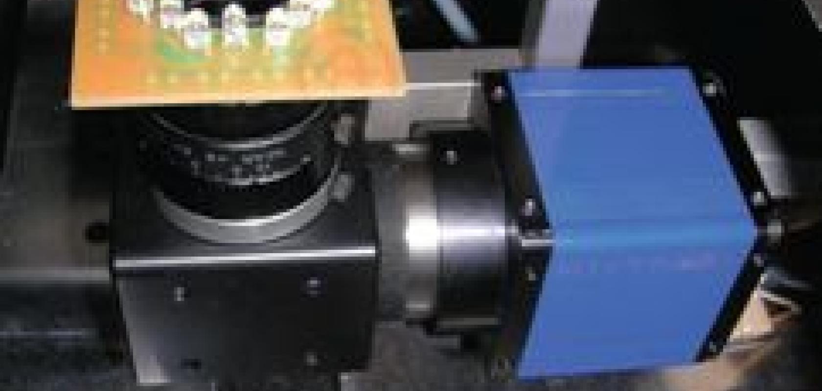
Matrix Vision’s mvBlueFox USB camera is part of an electronic component handling system from German company, Amadyne. The system is used for, among other processes, die bonding – whereby the semiconductor die is attached to its package or to another substrate. The sensitive components, with edge lengths ranging between 200μm and 400mm, have to be placed very precisely in housings or on boards.
‘The challenge in any electronics manufacturing environment is the range of components involved,’ comments Bleise. Electronics manufacture will involve hundreds of thousands of possible parts to be placed and there generally is no standard in terms of what a specific component looks like. For example, a tantalum capacitor can be any number of different colours, from beige to black, which makes it very difficult for standard colour inspection to identify the part. Therefore, robust algorithms must be in place that are capable of identifying the component through its geometry. ‘This type of inspection requires a high-quality camera along with the correct illumination,’ Bleise says.
And it’s the illumination that Bleise considers as generally being the core issue with electronics inspection. ‘A contrast between a pass and a fail is relatively difficult to achieve in the electronics industry because of the variance in components,’ he says.
For different measurements, images are taken under different illumination scenarios to extract different properties, such as polarity, positioning, and surface integrity. To determine if a component is white, for instance, it would be illuminated from above with a camera capturing the reflected light, whereas darkfield illumination or backlighting is much more effective for determining the position of the component using edge detection algorithms, where possible. Illumination also depends on the material and for a shiny surface – a polished wafer for example – darkfield illumination is more suitable.
Bleise also notes that the stability of the imaging system is key in electronics inspection. As LEDs age, the light intensity decreases and therefore the imaging system has to be calibrated to account for any differences caused by this.
High-speed inspection
‘Electronics assembly is essentially a high-speed vision application,’ Bleise comments. Throughput of components is rapid, and if two or three images are taken at each station, this is a huge amount of image data that needs to be processed. In addition to carrying out the inspection, the system must be able to flag a flawed component and potentially correct it in the short window of time available. The mvBlueFox used in the Amadyne system contains a hardware real-time controller that synchronises the illumination and image acquisition and allows very fast image capture, which is vital for the high-speed imaging.
A concrete example of the rapidity of electronics manufacture is illustrated at Tyco Electronics’ Guangdong manufacturing plant in China, which produces electronic and electric components, including connectors and cable assemblies, at a production yield of 1,000 sets of equipment per day and a rate of up to 1,200 parts per minute. Due to the high-speed nature of the production process, random in-line inspection was conventionally used to inspect parts for defects. However, this method ultimately generated waste and therefore a vision system from Cognex was implemented to provide 100 per cent in-line inspection and reduce the number of rejects further down the production line.
As Cao Wuxiu, senior vision engineer of Guangdong Tyco Electronics Stamping Department, says, machine vision has already been used within the production process for eight years for quality control. ‘In conventional quality control, the product quality is primarily monitored via random inspection; therefore, it is difficult to detect some intermittent shortages of quality,’ Wuxiu says.
Cognex’s In-Sight 5100 vision system, implemented by Cognex’s partner, Shanghai Ximing Vision Technology, was used to provide 100 per cent in-line inspection. A telecentric lens was also used to overcome the large scene depth involved in production process. All sizes of products could be tested in order to judge whether they lack a pin – the most common defect – and the inspection platform was set up to collect flawed product data and display a size and trend chart of all products on the interface.
Wuxiu states that using the new system, costs can be reduced through improved quality control, and because the vision system provides 100 per cent in-line inspection, product defects can be identified at an early stage and product rejection can be kept to a minimum. At the same time, the condition of the production device can be indicated via the inspection data of the vision system, thereby providing product stability through being able to replace parts when defects arise.
The highly automated production processes present in the electronics industry have meant that machine vision is relied upon heavily for placing parts and as an inspection tool. In addition to cameras for inspection, vision is also used in the form of barcode or data matrix readers for traceability purposes, as many components will contain some form of unique identifier. The range of imaging techniques required will continue to grow and machine vision will be a key part of electronics production as components and circuit boards continue to shrink in size.