When Christmas arrives, many a stocking by many a fireplace will be stretched to accommodate the latest consumer gadgets, be they flat screen TVs, laptops, consoles, or smartphones. Santa does, however, have a budget – and consumers of electronic devices are mindful of the price/performance ratio of their toys; they want reliable devices that are an improvement on last year’s model while costing less. For the manufacturers, this means that devices such as flat panel displays must be produced on ever-larger production lines, with ever-greater economies of scale, with the same accountability, reliability, and cost-effectiveness. Reliability means checking, and checking small features on such high-throughput production lines usually means line scan cameras. Consumer expectations, therefore, are passed right up the supply chain, even as far as machine vision suppliers providing the means of meeting these expectations.
‘The demands on line scan cameras are growing all the time,’ says Martin Wäny, chief executive of Awaiba (Funchal, Portugal), a machine vision company that produces line scan sensors for industrial inspection applications. ‘As features in LCD displays and high-end PCBs are getting smaller and smaller, the throughput speed has to be increased constantly to curb the cost of production. It all combines to mean ever-increasing requirements for speed and resolution at the inspection stations.’ High-end PCBs such as those used with fl ip chips, he says, have features as small as 5μm, which means that inspection equipment must be capable of imaging very high resolution to be able to spot defective parts. Despite the shrinking features on modern PCBs, reducing the throughput speed of a production line to allow more thorough inspection is not an option. ‘Rather, the pressure is always for it to be increased,’ he says. ‘The same trend holds true in the fabrication of the latest generation of LCD and LED displays.’ The exposure time for each line of pixels in a line scan camera can be as short as a few microseconds, meaning that blur-free high resolution images can be acquired even when the product is moving at high speed.
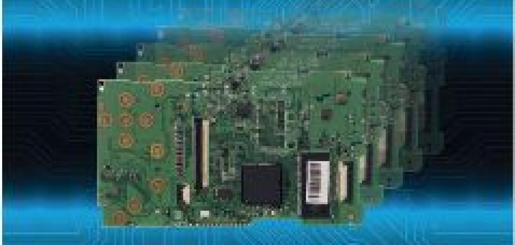
Xing-Fei He, senior product manager at Dalsa’s R&D facility (Waterloo, Ontario, Canada) explains that as manufacturers of flat panel displays upgrade their factories, they end up dealing with larger and larger pieces of glass. The current 10th generation (or G-10) flat panel display fabs are capable of dealing with glass substrates measuring 2.88 x 3.13m. ‘Normally we’d need 20 or 30 line scan cameras in a single system [for a G-10 factory], and the large number of cameras leads to a high cost in terms of lenses, cables, and other optics,’ says Xing-Fei. ‘It’s a headache to manage this large number of components from a design point of view, and so the major OEMs are always looking to reduce the number of components, starting with the number of cameras.’
Xing-Fei explains that the obvious way to reduce the number of line scan cameras required to inspect a production line of a certain size is to increase the number of pixels on each camera. ‘Dalsa now offers the Piranha HS 12k, a 12,000-pixel line scan camera with a small pixel size of only 5.2μm, and so for every three 8k cameras our customers are using, they can now use just two 12k cameras,’ he says, adding that 8k (8,000-pixel) line scan cameras represent the current industry standard in flat panel display inspection. Reducing the number of cameras, he says, also reduces cabling costs and downtime due to maintenance. Other manufacturers have also released higher resolution cameras, such as the Dragster line from Awaiba, offering up to 16k pixels. Dalsa has also recently released a 16k line scan camera.
Coping with more bandwidth
Progress in one branch of the technology tree does, however, demand developments in its neighbours: increasing the number of pixels per camera reduces the total number of components required, but it also means that each camera produces more data. The HS 12k, for example, operates at a line frequency of 90kHz, which corresponds to a data rate of 1.08GB/s, which is beyond the bandwidth limitations of most existing interface standards. Mark Williamson, sales and marketing director of Dalsa’s distributor Stemmer Imaging (Tongham, UK), elaborates: ‘Line scan applications are probably the biggest driver for the new Camera Link HS standard that’s in the wings at the moment. Line scan for high speed applications is actually driving the interface technology.’ The Automated Imaging Association (AIA) is completing the development of the HS Link interface and Dalsa’s current HS Link cameras will become Camera Link HS cameras once the standard is approved.

A 16k line scan CCD sensor produced by Awaiba
The current family of HS Link cameras are capable of approximately 1.5GB/s and cables can go to 15 or 20 metres at full speed, whereas Camera Link has a maximum bandwidth of about 850MB/s and only five to 10m cable lengths. Camera Link HS will, Williamson says, be able to go as high as 6GB/s. ‘We’re only just scratching the surface of what Camera Link HS will be capable of. At the high end, I think that line scan behaves a little bit like Moore’s Law with processor speeds. In another two years, when the resolution of flat panel displays gets higher, they’re going to want to do more imaging in the same time.’ The new standard, he adds, will have the capacity to cope with these demands.
Balancing exposure
Print and web inspection represents another significant application for line scan cameras. Here too, the trend to higher and higher line scan speeds means that the exposure time allowed for each pixel, already in the order of microseconds, is getting shorter. With so little time to gather the photons required to form an image, obtaining adequate illumination becomes challenging, and can even become a limiting factor in itself: ‘Dalsa does not produce light sources,’ says Xing-Fei. ‘If our customer cannot find a bright enough light, there’s no point in developing a higher speed line camera.’
Fortunately, such illumination does exist. Traditionally, the brightest lights available for machine vision applications have been incandescent metal halide bulbs, usually housed away from the workpiece with fibre optics to deliver the light. LED illumination has developed to the stage that it is competitive with metal halide bulbs in terms of brightness, while offering the cost and reliability advantages characteristic of solid-state technology. Simon Stanley, managing director of ProPhotonix (Cork, Ireland – formerly StockerYale), describes some of the ways in which this is achieved: ‘We work with chip-on-board technology, which means that we take an LED chip – the semiconductor chip – and we package it ourselves, either to make our standard products or custom products. In contrast, most other lighting manufacturers work with pre-packaged LEDs,’ he says, adding that the company’s chip-on-board modality offers significant advantages over ready-packaged chips, particularly for line scan applications. ‘We can make a very dense array of LEDs. If you think about what you’re trying to do with line scan, you’re essentially looking at a line of product, be it a web, a piece of glass, or a semiconductor. We want to illuminate that line in the field of view of the camera as evenly as possible, and we can do that well because of the very high density of the LED chips.’

ProPhotonix’s Cobra high density LED illumination for line scan applications ensures that even microsecond exposures obtain sufficient exposure
In a 100mm strip, Stanley says, the company can place 160 LEDs – while a more conventional approach would only manage 10 or 20 LEDs in the same space. ‘That’s really the power of our technology, and that’s the engine behind the Cobra product line,’ he says, specifying that this product line was designed to outperform metal halide-based illumination products. ‘Most people will agree that it was amongst the first products out there that could actually compete with halogen-based and fibre optic-delivered illumination.’
While the cameras in a line scan system can be mounted at some distance from the surface, the illumination must be quite near to it. The surface under inspection will, in many cases, be heat sensitive, and so ProPhotonix must ensure that heat is dissipated efficiently from the light source. Careful use of heat sinks and fans can, says Stanley, achieve the desired results, but custom applications may require customised solutions.
Customisation requirements aside, Stanley states that, for a vendor in the line scan market, the scalability of linear products offers certain advantages: ‘It’s very nice, from a business perspective, that we can make this single module and sell it at 300mm long for the semiconductor industry, but we can also sell it at two or three metres long for integration into a paper mill.’ Not only do the LED products offer an attractive replacement for metal halide bulbs, but they offer capabilities that would not be possible with the legacy technology: ‘Most customers tend to use a continuous light,’ says Stanley, ‘and if they’re using halogen bulbs they have no choice but to use continuous. We’ve had people come to us looking to synchronise the light with the cameras – they want to strobe it. They can also alter the colour of the light, two or three colours in one line, so as to help with the contrast.’
There are some applications, however, where very high brightness lighting is not a viable option – in scanning photographic films or when working with particularly heat sensitive materials. In these applications, the technique of time delay and integration (TDI) can be used to increase the sensitivity of the sensor while keeping read noise low. Xing-Fei from Dalsa explains that rather than having a single line of several thousand pixels, sensors intended for this technique have up to 256 lines. ‘You move the sensor over the object in such a way that the object moving forwards is synchronised with [the charge in] each line of the 256-line CCD,’ he says. As the charge corresponding to one part of the subject moves through the CCD, it is exposed once for each line on the sensor (up to 256 times on some devices) before being converted to a signal at the output. ‘It’s important to note that the charge is summed in the charge domain, and only read out to the digital domain at the very end.’ This, he notes, means that noise associated with reading the signal is only introduced once for those 256 exposures. The technique is used in many low light line scan applications.
The CMOS approach
As has been the case in area scan technologies, CMOS has found a place in line scan applications as a high-speed and cost-effective alternative to conventional CCDs.
Joachim Linkemann, product manager at Basler Vision Technologies (Ahrensburg, Germany), compares the characteristics of a CMOS sensor for line scan with those of the conventional CCD sensor: ‘Usually CMOS is expected to have high noise and a high threshold for seeing the first signal, and these are disadvantages, but the huge advantage is the speed that you can achieve with CMOS. Therefore Basler has developed a CMOS with a low read noise and a low threshold, and which is also very fast.’ The device is capable of 140kHz on a 4k line, which corresponds to 560MB/s.
According to Martin Wäny of Awaiba, sticking with an established interface technology like Camera Link offers certain advantages, despite the fact that the company’s highest speed 16k cameras must use two such cables. ‘This interface solution is not optimal, but it is the most pragmatic solution as long as there is no clear sign for the next higher-speed camera interface,’ says Wäny. ‘Customers are reluctant to opt for either of CoaXPress or HS Link, as it is not yet clear when and if they will be adopted as industry-wide standards.’
In conclusion, there will always be a pressure for the developers of line scan cameras to enable higher speed, higher resolution inspection. The next generation of consumer electronics will cost less than the current generation, and will be produced to higher precision; it only remains to see which technologies the machine vision industry adopts to meet these demands.
-
Awaiba: www.awaiba.com
-
Dalsa: www.dalsa.com/mv
-
Stemmer Imaging: www.stemmer-imaging.co.uk
-
Automated Imaging Association: www.machinevisiononline.org
-
ProPhotonix: www.prophotonix.com
-
Basler Vision Technologies: www.baslerweb.com
