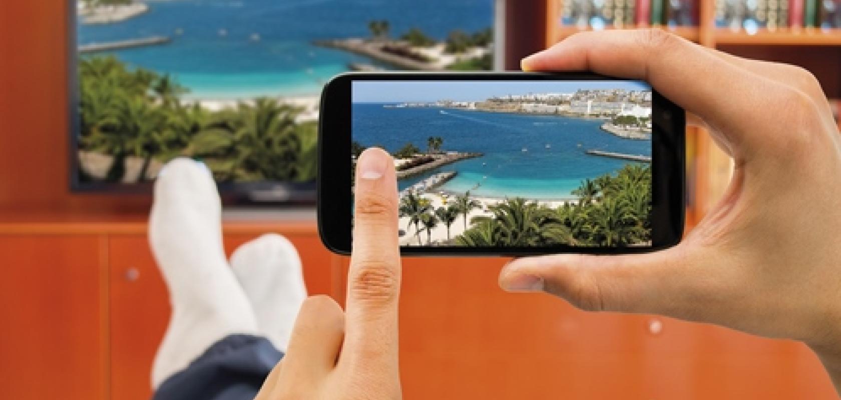
Screens for consumer devices have grown in size and resolution over the past decade, to the point where displays offering ultra-high definition (4k or 8k resolution), organic LED (OLED) or quantum dot LED (QLED) features are now commonly seen in our homes or our hands. Inspecting these high-resolution displays presents a number of challenges, the main one being that as pixels get smaller so do the size of the defects. In addition, for OLED displays in particular, which differ in composition to LCDs, new kinds of defects can occur that require new methods of inspection.
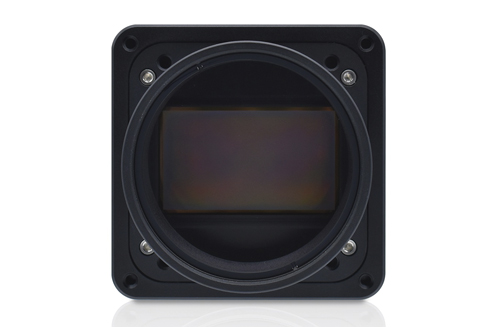
At the recent UKIVA Machine Vision Conference in Milton Keynes, UK, Wojciech Majewski, sales director for the optical imaging division of Vieworks, based in South Korea, discussed a 155-megapixel CMOS area scan camera with a wide field of view that the firm has developed to address the increasing demands of flat panel display inspection.
Known as the VC-155, the camera is able to run at 15fps at 8 bits and 7.5fps at 12 bits with a rolling electronic shutter. Majewski explained that the camera is used to inspect FPDs once the multiple layers used to produce them – for example the filters, glass and metallic mesh – have all been combined.
The 155-megapixel resolution of the camera is roughly five times that of modern mobile phone OLED displays, like those found on the Samsung Galaxy S8. This makes the camera suitable for detecting defects such as glass markings or faulty pixels. Vieworks’ annual report confirms that the firm’s customers include Samsung Electronics, in addition to other major FPD manufacturers.
The wide field of view of the VC-155 means that the entire display is captured in one image, rather than needing multiple images with lower resolution cameras. ‘Taking multiple images wastes a lot more time when inspecting mobile displays, as the camera needs to be mechanically moved before each picture is taken,’ Majewski said. ‘Time is money when you are producing 50 to 80 million mobile phones of a particular model.’
While the primary use of the VC-155 is inspecting mobile displays, according to Majewski, the camera can also be used to inspect televisions. Here multiple images are required; however, thanks to the camera’s high frame rate it can be moved over the surface at higher speeds, compared to alternative solutions with lower resolution and frame rate.
Other high-resolution imaging solutions have emerged recently targeted at FPD inspection. For example, at the end of 2017 Teledyne Dalsa unveiled its 86-megapixel Falcon4 camera operating at up to 16fps, while towards the end of last year Gpixel announced its 65-megapixel CMOS sensor and On Semiconductor a 50-megapixel CCD sensor. In June Canon USA also revealed a 122-megapixel CMOS sensor that can operate up to 9.4fps.
InZiv’s nano-optical inspection system for R&D and quality assessment integrated with an optical inspection system
‘As past trends have shown, there will always be a need to make larger, higher-resolution cameras,’ said Majewski. ‘For our demanding customers, even while the 155-megapixels we offer at 15fps has satisfied their demands for a period, this isn’t enough to satisfy their demands in the future. They are already asking for faster, bigger cameras, which I can confirm will be coming in the future – so the trend will continue.’
Rising resolutions
The majority of high-end televisions and mobile devices are now equipped with OLED displays. According to Majewski, the biggest problem in OLED display inspection is encountered when examining how well the displays emit very low levels of light. ‘Here we encounter what is called Mura – a Japanese term used in the display industry to describe non-uniformities,’ he said. ‘The human eye is very sensitive to Mura when OLED screens are displaying high grey or black levels; therefore it is crucial that such non-uniformities are identified by our cameras during quality inspection.’ One of Vieworks’ other high-resolution cameras, the VP-151, offers 151-megapixel resolution and 78dB of dynamic range, which make it capable of capturing these Mura and other small defects in detail, according to Majewski.
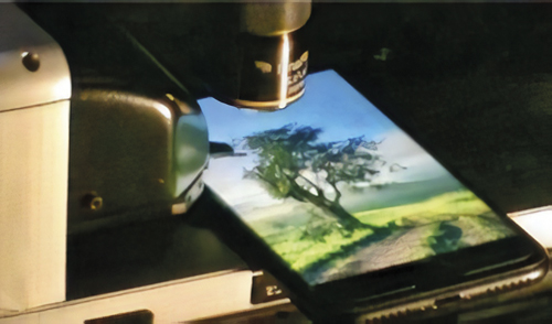
Display manufacturers also want to be able to spot defects formed during the deposition of organic material in OLEDs, which are potentially smaller than the diffraction limit of visible light. Israeli firm InZiv was founded six months ago to provide inspection tools for the FPD industry and, as of January, had raised $2.5m in series A funding.
‘We all came from a company which was an expert in the field of nano-optics – the ability to image light on the nano-scale – where the primary focus had been providing R&D systems for academia,’ David Lewis, CEO of InZiv, said. ‘When we saw the problems in the display industry, however, we realised that this technology holds all the critical elements to be a game-changer in the [FPD] field.’
According to Lewis, the object resolution of camera-based solutions for self-emitting displays is capped at around 1µm or larger – because of the diffraction limit of the imaging technique – meaning there’s nothing available in this field capable of imaging below that scale.
This creates issues, particularly when inspecting OLED displays, for which display manufacturers face a variety of challenges in depositing the organic material in a way that is even and without defects. Deposition defects are hard to see using standard optical techniques, Lewis said, adding: ‘Beyond the resolution, the optical techniques offer only 2D information, meaning they provide very little information about the 3D topography of the material deposition.’
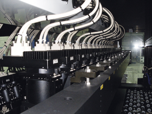
Large flat panel display inspection requires multiple high-speed cameras. Credit: Teledyne Dalsa
While details of InZiv’s technology remain sensitive at this time, Lewis confirmed that the firm’s new inspection solution ‘can be used to obtain: the height information of a defect down to sub-nanometre resolution; spectral information – the wavelength of light being emitted from each measurement point in a pixel; refractive index; and the type of material involved in a defect. All of this can be used to determine where in the manufacturing process a defect originates. This information cannot be obtained with a camera.’
The solution offered by InZiv is not only able to detect the nature of defects, but can also be integrated into existing high-resolution camera-based solutions to deliver a display inspection platform capable of identifying both the location and type of defects present in displays. The camera is used to perform a scan of the phone display, revealing any problem areas, which can then be inspected at higher resolution with InZiv’s solution to identify the type and origin of the defect.
‘Our technique can provide manufacturers with a very accurate map of the 3D topography, combined with super-resolution optical imaging,’ Lewis stated. ‘Our technology is camera-agnostic – it can be coupled with any type of camera-based inspection solution. At this stage, we integrate with any camera supplier, rather than producing our own camera technology.’
The solution offered by InZiv is capable of inspecting a full phone display. However, the firm’s goal for the future is to reach a point where it can inspect multiple phones on one panel, according to Lewis.
The technology is still very young. ‘Currently, it is more suited to the early stages of FPD development, where the OLED technology itself is still being worked on in R&D,’ Lewis said.
There has been a lot of interest in InZiv’s technology, according to Lewis, because the current yields in the OLED display market are very poor compared to LCD, which contributes to the high price tag associated with OLED technology. ‘The lack of ability to identify the origin of many defects is leading to a lot of problems, in terms of yield in the [OLED] display market,’ he explained. ‘It is clear that existing inspection solutions today are not enough to effectively deal with the problem.’
Reflecting on glass inspection
Glass inspection has its own difficulties, because it can be both transparent and highly reflective. However, when used at certain angles and with certain lighting conditions, manufacturers can use TDI cameras to detect any impurities or defects present in the material. The TDI cameras offered by Vieworks are able to achieve 18k and even 23k resolution with line rates up to 250kHz.
‘Vieworks TDI cameras use hybrid sensor technology, which means we use a CMOS chip structure integrated with a CCD on top, giving us the best of both worlds,’ Majewski said. ‘It combines the low signal-to-noise ratio and high dynamic range of the CCD – as well as the ability to move charge from one CCD line to another, to avoid additional noise – with the high readout speed of the CMOS.’
The advances that have taken place in polarised imaging over the past two years also show particular promise for the inspection of glass in FPD production – stresses in the glass can be seen under polarised light.
In 2018, Sony Semiconductor Solutions released a CMOS sensor for imaging polarised light, which has since been integrated in cameras from a number of suppliers, including Teledyne Dalsa. Dr Xing-Fei He, senior product manager at Teledyne Dalsa, said that imaging polarised light could be used to improve the inspection capability of FPD production lines, particularly where glass is involved. He also pointed out that the technology isn’t yet fully developed: ‘The technology is still very young and it needs a lot of improvements, for example an increased contrast ratio of the polarisation filters, but we think that this will be a trend in the future that imaging will be going through.’
Three fields, one capture
Because of the size of potential display defects decreasing with pixel size, according to He the traditional imaging methods previously used to detect display defects are no longer relevant, and because of this the industry is moving to a new technique, multi-field imaging.
‘Display manufacturers have previously been required to use bright field, dark field and back light images to inspect certain defects in displays,’ He said. ‘Previously, these images had to be captured in three separate scans, which took a relatively long time to do, making it more difficult to meet the time restrictions of the production line.’
The perfect diamond structure of this OLED screen of a Samsung Galaxy can be seen after being captured using a 151-megapixel camera from Vieworks
For this reason, the Linea ML line scan camera launched by Teledyne Dalsa last year – in addition to its upcoming Linea HS TDI line scan camera – has been designed to capture bright field, dark field and back light images in a single scan, which speeds up FPD inspection.
‘Multi-field imaging is enabled by using either time division or wavelength division. Here, a special coating on silicon creates a colour filter that separates different wavelengths, which have different lighting angles, and that are used to capture the three different types of image,’ explained He. ‘The challenge with multi-field imaging, however, is that because all three types of image are captured at the same time, a higher level of data throughput is required to process them in the reduced time frame enabled by using the technique.’
To meet the increased data throughput requirements of multi-field imaging, Teledyne Dalsa developed Camera Link HS, which incorporates fibre optics. The high-speed interface enables the Linea ML and upcoming Linea HS camera to transmit data at 5GB/s, according to He, approximately six times faster than the data transfer enabled by the traditional Camera Link interface.
Multi-field imaging is a feature offered by Vieworks’ TDI cameras, with the firm planning to release a system in 2020 equipped with it.
Going micro
An interesting development in the consumer display market has been the emergence of micro-LEDs, a technology poised to rival OLEDs and QLEDs that Samsung demonstrated at the Consumer Electronics Show two years in a row – first as a 146-inch display called The Wall in 2018, then a 75-inch television display.
Pixels based on micro-LEDs consist of arrays of microscopic LEDs forming each individual pixel element. As is the case with OLED pixels, micro-LED pixels produce their own light – rather than requiring a backlight such as those found in LCDs – meaning they are able to achieve the perfect black levels currently associated with OLEDs. They can also do this without the danger of burn-in – an issue that has plagued OLED displays since their arrival, where persistent images on-screen remain faintly in the background even after the image changes. In addition, micro-LEDs have been shown to deliver a longer lifetime than OLEDs, a higher brightness than any current display technology, a wide colour gamut, all while avoiding issues regarding viewing angle and uniformity faced by LCDs.
While the technology shows promise, and despite Samsung having announced it will offer micro-LED displays to the home luxury market by the end of the year, the technology is still in its infancy.
Vieworks’ VC-155 camera offers 155-megapixel resolution and a wide field of view, enabling it to capture an entire phone display in a single image
As to how the emergence of this potentially disruptive technology might affect the demands placed on imaging technology used to inspect it, even with the new pixel structure, He, of Teledyne Dalsa, doesn’t believe there will be a significant change. ‘The pixel size might get smaller, and the type of defect might be different, but in terms of inspection I don’t see it needing a specific technique,’ he said.
Teledyne Dalsa does currently have some customers inspecting micro-LED displays. However, these are large displays intended for outdoor use, such as advertising, rather than in smaller devices for consumer use. The pixels of these displays are also much larger than those that would be used in televisions, phones or tablets.
Lewis, from InZiv, had a slightly different opinion: ‘Every new technology brings with it new challenges. When the semiconductor industry went from the microscale to the nanoscale, a whole new field of tools were needed to deal with that. I think we’re starting to see the same transition occur in the display industry, but up until now, the resolution hasn’t been so challenging that this was really a strong issue.’
He added that the same aspect that makes InZiv’s solution valuable to the OLED industry – the ability to give a wide variety of information at the nanometre scale – will make it equally important for micro-LEDs.
![]()
Teledyne Dalsa’s Linea ML line scan camera can perform multi-field imaging, enabling it to speed up inspection of FPDs
Examining electronics
Imaging in 3D is a valuable tool for examining printed circuit boards (PCBs) for defects such as missing solder joins, excess solder paste, rotated, misplaced, or even missing components.
Dr Athinodoros Klipfel, sales manager for 3D sensors at Automation Technology, described how one of the firm’s OEM customers used its 3D imaging technology, in combination with a colour line scan camera, to inspect surface mount device (SMD) assembly on PCBs.
The system was able to identify PCB defects, such as if multiple microchip pins had mistakenly been soldered together, or if an SMD component had been soldered out of alignment relative to other components.
‘Around four years ago this customer was only using the line scan camera to inspect PCBs. However, this prevented them from detecting certain defects as they lacked depth information, meaning their machines weren’t as reliable as they could be,’ said Klipfel. ‘Now, using our 3D sensor, they have been able to increase their machines’ capability to detect defects and increase their reliability, providing added value to their customers.’
A point cloud image of a PCB obtained using 3D imaging. Credit: Automation Technology
Imaging in 3D has been used for PCB inspection for at least 15 years, according to Klipfel. However, compared to 15 years ago, a number of developments have taken place that have greatly increased the capability of the technology, one of which is blue lasers becoming more affordable. Blue lasers produce a thin scan line and generate a low amount of speckle, which reduces noise in the 3D data and improves resolution.
There are also now larger sensors – Automation Technologies’ 3D cameras can generate more than 4,000 data points per line – that operate at higher speed. Klipfel said that inspecting larger PCBs, such as motherboards for computers, takes around 10 seconds using the company’s 3D sensor, whereas it takes two to four seconds to inspect smaller PCBs in mobile phones.
Looking to the future, Klipfel said Automation Technology is not only working on further increasing the speed of its 3D sensors, but also looking to take advantage of developments in illumination technology that will lead to better laser beam quality and straightness of laser lines used for 3D imaging.