Growth in solar has, to date, largely been political, reliant as it is on government subsidies and incentives. The market has been a strong source of revenue for machine vision and even during the 2008 recession, when other industrial sectors were crumbling, it remained a lifeline for many vision companies. Last year photovotaics saw a boom, with worldwide PV installations reaching a record high of 18.2GW, a growth of 139 per cent Y/Y according to figures from solar market research firm, Solarbuzz. However, the organisation predicts a 14 per cent contraction in the European PV market in 2011 in its latest report, while the US PV market is set to double in 2011.
So what advantages does machine vision bring to solar cell production? Gregory Hollows, director of machine vision at optics and imaging company, Edmund Optics, comments: ‘Machine vision came into play as the [solar] market has matured to automate processes and bring costs down, especially for something as expensive to manufacture as photovoltaics. Automation is very important for both accuracy and cost reduction, and imaging has been a part of solar cell production for a number of years.’
The dominant photovoltaic technology is crystalline silicon solar cells, which accounts for around 80-90 per cent of market share. The remaining 10-20 per cent is made up of thin film solar cells. Crystalline is the more mature technology and produces the highest efficiencies (up to 20 per cent for monocrystalline cells), while thin film still has some catching up to do in terms of efficiencies, but is cheaper to manufacture and more suitable for high-volume production.
In crystalline silicon PV production, inspection begins immediately with the raw silicon ingot, which is checked for impurities and inclusions. Silicon is transparent in the near infrared, meaning that infrared cameras can see through the block of material, which can be more than 10cm thick. Raf Vandersmissen, CEO of sInfraRed, a Xenics subsidiary based in Singapore, comments that the company has sold a lot of shortwave infrared (SWIR) cameras for ingot inspection. ‘The aim is to inspect the ingot for impurities or voids,’ he explains. ‘You can detect silicon carbide, for example, which can form in the silicon and which is not only an unwanted impurity but, as it’s a very hard material, can also cause damage to the saw when the ingot is cut.’
The silicon is then sliced into very fine wafers, around 100-200μm thick. These are sorted optically and electrically. Thickness is measured with sensors like the CHRocodile IT from Precitec (available in the UK from Armstrong Optical), a sensor based on laser diode technology. The sensor can measure thicknesses from 18μm to 3mm in air with a resolution of better than 60nm for silicon.
One of the more important optical tests is the detection of micro-cracks in wafers, which could lead to the wafer breaking further along production and potentially shutting down the line in order to clean it. This costs money. Guido Eberhardt, sales manager at Isra Vision (Darmstadt, Germany), states: ‘If you can improve production uptime by half an hour per day, that’s a lot of money saved.’
Isra Solar Vision, a business unit of Isra Vision, produces optical inspection systems for solar cell manufacture. Its SolarScan product line is designed for crystalline solar cell production, while the PowerScan line caters for thin film inspection.

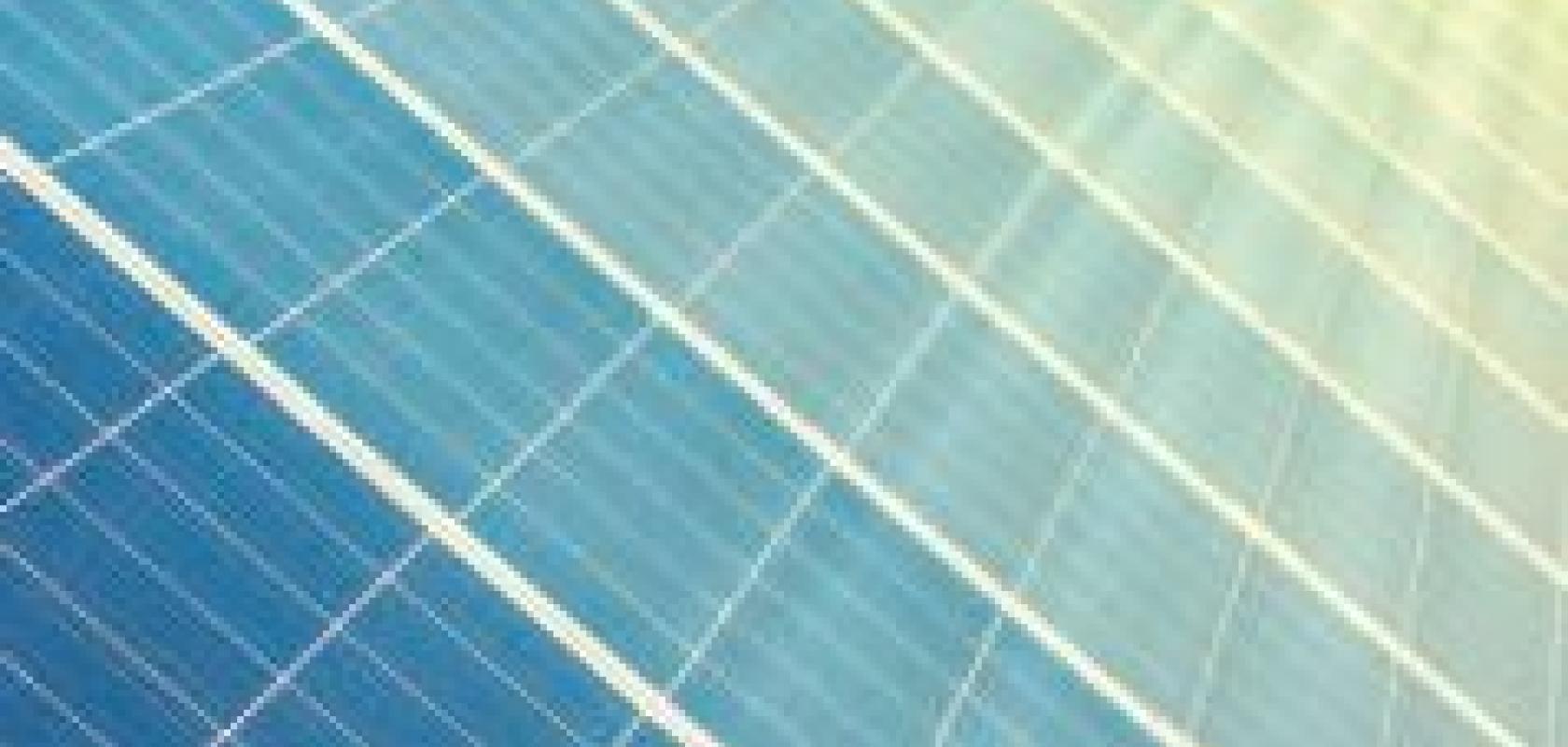
Solar cells are sorted according to efficiency, colour, print quality and defects detected by luminescence testing. Image courtesy of Isra Vision
Vision is also used to classify the different types of micro-crack. ‘Most cells will contain micro-cracks in some form. Inspection will concentrate on identifying those micro-cracks that are deemed critical,’ explains Eberhardt, adding that the critical forms are those that extend to the edge of the wafer, which could be the start of a break.
In addition to the wafer being very thin, force is applied to it during processing, which makes weeding out those wafers with critical micro-cracks all the more necessary. Xing-Fei He, senior product manager at Teledyne Dalsa, says: ‘This problem, in having to handle such thin wafers, is unique to photovoltaics production.’
Micro-crack inspection uses back-lit near-infrared illumination rather than visible, as silicon is semi-transparent in NIR, but opaque in the visible region. While infrared cameras are an option, they are expensive and are limited in resolution, and so most solar manufacturers will use cooled, silicon-based CCD cameras that have some, if minimal, responsivity at around 1μm. Because the responsivity is low – at 1μm CCD cameras are limited by the bandgap of silicon – longer integration times are used: ‘A typical area scan camera would take around 300-1,000ms to capture the image because the quantum efficiency is so low at this [1μm] wavelength,’ explains Xing-Fei.
For micro-crack inspection, Teledyne Dalsa provides line scan TDI cameras that go some way to overcoming these low quantum efficiency (QE) values. TDI is a technology that enables multiple exposures to be taken to acquire an accumulative image. This provides higher responsivity even with a low QE. For example, Teledyne Dalsa’s Eclipse and Piranha TDI cameras have 96 stages, meaning the scene is exposed 96 times, summing up in the charge domain from each exposure.
‘The alternative to a TDI camera is an InGaAs camera,’ states Xing-Fei. ‘These cameras are more expensive and have some limitations in resolution, which means more cameras are required to make the inspection, and that increases the cost. The major issue with InGaAs cameras for micro-crack inspection is the cost.’
Luminescence measurements
The properties of silicon mean that when excited, either electrically or with photons, it luminesces with a relatively broad signal at around 1,150nm, as the silicon acts as an inefficient LED. This luminescence from silicon can give diagnostic information on how efficiently the cell is operating. Two inspection techniques are employed: electroluminescence (EL), whereby the silicon is excited electrically, and photoluminescence (PL), which uses photons of light to excite the cell.
‘Instead of creating a current from incident light on a solar cell, these inspection techniques work in reverse, measuring the light produced by the silicon,’ explains Vandersmissen of sInfraRed. ‘The fact that silicon has this luminescence effect around 1,150nm is just a physical feature of the material.’
The test measures the amount of light produced by the solar cell; the more light generated, the more efficient it is. The inspection system will also identify cracks within the cell, which will appear as a black line in the image.
‘The advantage of the luminescence technique is that it will give an idea of not just whether the cell is good or bad but also which area of the cell is good or bad,’ Vandersmissen continues. Xenics and sInfraRed provide SWIR cameras for luminescence testing, although Vandersmissen admits most commercial inspection systems still work with cooled CCD cameras because of their higher resolution and lower cost. Integration times with CCD cameras are longer compared to SWIR, he points out.
However, research centres interested in classifying defects do typically require SWIR cameras, Vandersmissen says, as the defects themselves might luminesce at different wavelengths further into the infrared.

Micro-cracks in the silicon wafer could lead to breakages and production downtime. Image courtesy of Isra Vision
Of the two tests used commercially, EL is simple to deploy, but can only be applied to a completed solar module, as it requires electrical contacts to be made and a complete circuit. PL, on the other hand, works through excitation of silicon with photons, typically from a laser or LED, and therefore can be used throughout production, right from testing the raw material. The disadvantage, however, is that it’s a more complicated setup – it needs an external light source and a high pass filter to filter out the reflected light from the illumination source to leave only the luminescence signal, which is relatively weak.
Vandersmissen notes that one way to move to higher resolutions with a SWIR system at an acceptable price is to choose a line scan camera. Recently, Xenics has introduced SWIR line scan cameras with a resolution of 1,024 or even 2,048 pixels per line. ‘If you sweep the camera over the entire solar panel or ingot, for instance, the 2,048 pixel line width would provide a very high resolution image,’ he says.
From wafer to module
There are numerous other processing steps to reach the final crystalline solar module and optical inspection plays a role at most stages. The wafers undergo surface structuring, doping to split them into positive and negative sides, and are coated with an antireflective (AR) coating.
The next step is a metallisation process to establish the front-side and rear-side contacts. The printing on the front side is inspected to ensure accurate alignment of print with the wafer edge (tolerances are typically around ±100μm). Eberhardt of Isra Vision comments: ‘Mechanical alignment could be used, but every time the cell is touched new defects are produced and manufacturers prefer not to use this method. Most alignment is carried out using optical information to match the position of the cell and print lines with the contacting unit.’
After printing the cells are dried and laser scribing or chemical etching (chemical etching is typically made before printing) to isolate the front from the rear side. Cells are then sorted, the primary criteria for which, according to Eberhardt, is efficiency, followed by colour, print quality and defects found from luminescence testing. Finally, cells are connected to form a module. ‘This cell matrix is checked one last time before lamination, because after lamination there is no possibility to change or repair anything,’ explains Eberhardt, adding that electroluminescence is typically used.
Xing-Fei of Teledyne Dalsa feels optimistic for vision technology for the photovoltaic market: ‘In the next 10 years, mass production of solar cells will increase, and AOI will play a key role, as there needs to be large-scale automation in manufacturing.’
Hollows of Edmund Optics categorises solar as a fundamental part of the electronics market. However, he says that in contrast to other electronic products, the question yet to be answered is whether solar panels are cost-effective enough for the market to continue to grow. ‘Without government subsidies, even the European market, which is traditionally more willing to deal with higher cost products, has had trouble sustaining installation growth,’ he says.
‘Automation is going to bring the price down, but solar panels are expensive to deploy – installing solar panels on a house in the US could cost $25,000. The question is, is there going to be a generational jump in the technology that’s going to double the efficiency or halve the cost? That’s when solar technology will go through the roof.’
In-series production of thin-film solar modules, being able to track individual processing steps is critical. The production facility of Schott Solar Thin Film (Jena, Germany) manufactures around 1,000 thin-film modules per day, which equates to a production capacity of more than 33MW per year. To ensure a reproducible high quality of solar modules, Schott Solar Thin Film employed the OCR (optical character recognition) 1D/2D code reading system, Simatic MV440, from Siemens and iiM AG.
The system was installed to read OCR markings from below. The serial numbers – lasered onto the layers of metallic back contacts – have some inherent blurring and are difficult to focus on and read. On top of that, the metallic surfaces are highly reflective when illuminated and the characters are low in contrast. ‘We solved these issues with a special arrangement of the optics and an optimised lighting,’ says iiM managing director Axel Müller.
In the past, the conveyors had to stop for barcode acquisition, since the scanners could only read at a standstill. Thanks to the short exposure times and the high light intensity, the code reading systems now read at full operating speed.
According to Schott Solar Thin Film, the MV440 systems also enable 100 per cent track and trace so that faulty modules can be removed.