Globally, the solar industry continues to be in dynamic growth, especially in China and Southeast Asia, with India rapidly becoming the main driver of the market. In the past few years, Isra Vision alone has installed, on average, a couple of hundred systems per year, 90 per cent of which were in Asia.
But the industry is also seeing ‘the signs of a renaissance of the solar industry in Europe’, according to Christian Probst, managing director Isra Vision – GP Inspect. ‘The war in Ukraine and the resulting political developments will accelerate growth,’ he says.
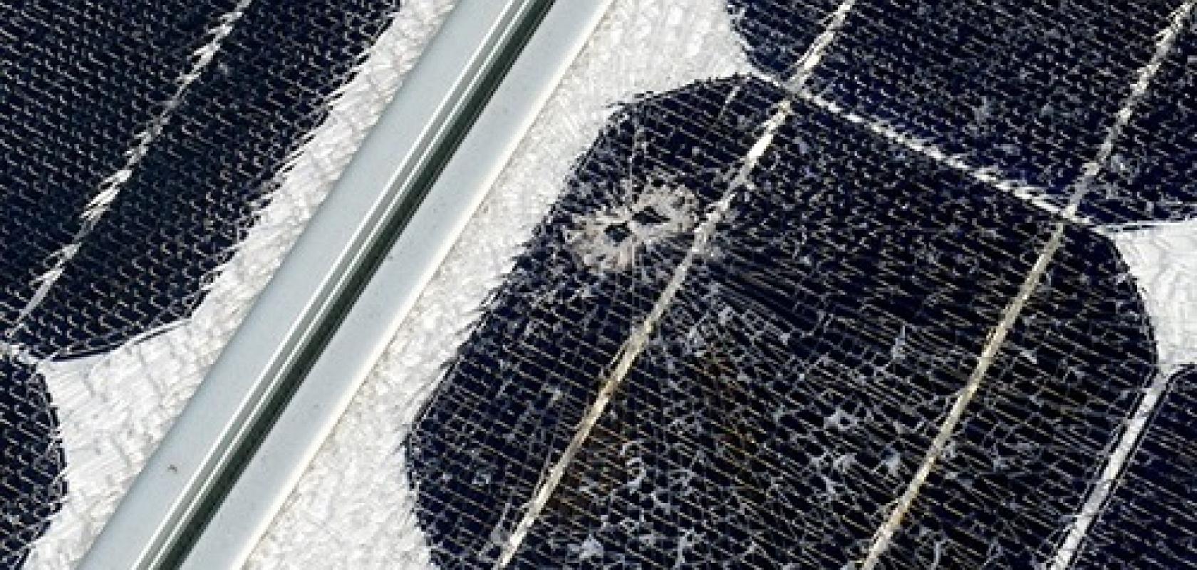
But even in the face of huge growth, the solar industry is not an area in which quality can be compromised. During production, inspection systems examine the surface conditions and geometry of the wafer, checking for distortion, cracks, chips and contamination. Microcracks can eventually cause an entire panel to shatter, causing possible knock-on damage to equipment and other panels in the array and requiring an expensive shutdown of the line for clean up and repairs.
It is therefore no surprise to hear from Xing-Fei He, senior product manager at Teledyne Dalsa, that ‘solar cell manufacturers are moving to 100 per cent inspection of each panel after every major processing step. They are under pressure to increase the quality of their products and reduce costs. Yield is critical, and optical inspection is a vital tool.’
Compare and contrast
‘The inspection of solar cells can take place at various stages of the production process,’ says Probst. ‘However, this also depends on the producer. Does it want to detect defective cells already within the process and reject them as quickly as possible? Or is a final inspection at the end of the production line sufficient?
The Isra Vision – GP Inspect portfolio starts with the incoming inspection for raw wafers, where they are checked for surface defects, microcracks or chippings. This is usually followed by texture monitoring, where the quality of the surface is reviewed after the chemical bath. Next comes coating inspection, followed by print and structure inspection on the front and rear sides, and the final cell classification and sorting.
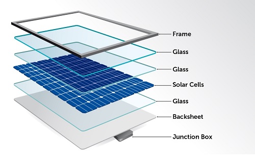
The different layers of a solar panel. Credit: TWI
Dr Jonas Haunschild, head of the inline wafer, process analytics and production control group at the Fraunhofer Institute for Solar Energy Systems ISE, says that one of the greatest challenges lies in characterising the many interacting thin layers that make up modern solar cells. Each of these layers must be controlled, preferably not only at one point but over the entire surface.
Probst agrees the fineness of the layers and the weak contrast between them makes inspection very challenging: ‘Different structures within the cell must precisely align with each other to achieve the highest possible efficiency. Meanwhile, these structures are so fine that the regions responsible for charge separation are only a few hundred micrometres apart. The patterns are only faintly visible and often have shallow contrast.
‘Depending on the layer, this is already very demanding, but we want to go one step further,’ explains Haunschild. ‘The processes to be developed should be so fast and so cheap they can be used in the production environment of solar cell manufacturers.’
Inspecting flexible photovoltaics
Back in 2018, 16 partners joined forces as part of the EU-funded OledSolar project to accelerate the widespread commercialisation of organic light-emitting diodes (OLEDs) with thin-film solar cells. Focused on developing innovative manufacturing, monitoring and inspection processes, the technologies developed during the project, which closed earlier this year, may help deliver new types of solar-powered devices, such as energy-efficient lighting, flexible display screens and solar panels that could be smoothly integrated into the structure of buildings.
TWI’s custom-designed relay circuit switches the power supply on and off according to the square wave generated. Credit: TWI
TWI, based in Cambridge, UK, was one of the project partners. Working closely with the project co-ordinators, VTT Technical Research Centre of Finland, TWI has been developing inline quality-control techniques for photovoltaic module production, with the aim of automating a defect detection method for roll-to-roll printed flexible solar cells, ultimately improving quality, yield, processing efficiency and sustainability.
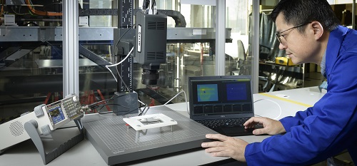
‘We developed our thermography system here at TWI and that was then taken to VTT to be integrated with its production system,’ explains Martin Bourton, principal project leader. It made sense for the TWI team to go for an approach making use of dark lock-in thermography (DLIT). Inspected parts are usually in thermal equilibrium. When it comes to photovoltaic materials, the main options for creating a thermal contrast between defects and the background material are either applying a current light source or introducing a new one. Both approaches can spread heat through the sample and muddy spatial resolution, but it was reasoned that voltage could be more easily regulated. This also worked well for VTT’s testing line.’
TWI’s DLIT system has proved a success in the lab and in field trials, where it has been validated on VTT’s roll-to-roll pilot line. The new approach identified sub-millimetre defects (appearing as hot spots) far more clearly than standard inspection methods. ‘The system looked at hundreds of pieces and successfully identified all the defects that had been artificially introduced onto the sample to replicate defective printing,’ confirms TWI’s senior project leader, Haitao Zheng.
When the electrical characterisation of the printed film begins, it triggers the synchronised thermography inspection by an infrared thermal camera located below the test area. TWI’s DLIT system applies a square wave current to heat the test film and a thermal image is produced, ready for post-processing.
TWI’s custom-designed relay circuit switches the power supply on and off according to the square wave generated. This enables high voltages to be applied using a low-voltage signal. As well as capturing thermal images, the camera also records the synchronised square wave reference signal created by a signal generator.
As well as capturing thermal images, the camera also records the synchronised square wave reference signal created by a signal generator. Credit: TWI
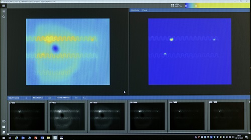
‘We also developed a graphical user interface software in-house, which provides thermography data acquisition, data visualisation, lock-in post-processing and data analysis capabilities,’ says Zheng. ‘When we compare our DLIT system to the standard approach, you can see there is far less background noise and our processed image shows defects very clearly.’
And the biggest challenge? ‘That has been the inline implementation,’ says Zheng. ‘DLIT is not as fast as standard inspection methods. It’s a stop-and-go inspection approach, requiring about 20 to 30 seconds between the input signal and post-processing.’
TWI is now looking to optimise the system to develop it into a commercial product, Zheng explains. ‘We’re looking to improve the speed, by developing a shorter input signal and programming the post-processing software in the C programming language, rather than using Matlab and Python, for example.’