In recent years, infrared thermography has become a popular solar cell inspection technique that enables manufacturers to detect hot spots and other anomalies that cannot be found by visual inspection.
There are a number of ways it’s used. Near infrared and shortwave infrared cameras, for example, are able to see cracks and other defects on the inside and opposite side of a silicon wafer or ingot. Longwave infrared imaging can also be used to inspect and monitor the integrity of cells configured into solar panels once they have been installed, commonly by employing a thermal imager to detect hot spots or dead cells.
Mike Grodzki, product manager for scanning products at Teledyne, noted that infrared cameras can also be used to test photovoltaic cells by techniques called photoluminescence and electroluminescence, both of which can highlight flawed regions in the solar cell. Photoluminescence uses powerful illumination to induce luminescence, while electroluminescence requires an electric current to be applied to the cell or module and the emitted light measured.
Dr Jonas Kornelius Haunschild, head of the inline-wafer, process analytics and production control group at the Fraunhofer Institute for Solar Energy Systems ISE, explained that solar cells are inspected inline at two major stages in the production process. The first is an outgoing inspection of wafers or an incoming inspection of cells.
At this stage, the raw silicon wafer is inspected to verify wafer specifications and discard poor quality material.
The second stage is during the current-voltage (I-V) tests of the finished solar cells before module production begins. ‘Depending on different companies, inspection is also done during processing, but these two are the most important ones,’ said Haunschild.
Transparent to infrared
For inspection of incoming cells, the team at Fraunhofer ISE uses three different infrared systems: infrared transmission, infrared reflection and photoluminescence imaging. Haunschild described the first system, infrared transmission, as a simple method that uses a camera to detect 1,400nm infrared light focused on each side of the wafer.
‘The wafer should be almost transparent to this wavelength – and so, in the images, defects, particles and cracks can be seen. Simple image processing algorithms catch the defects and the inspection system can sort them out,’ he said.
Haunschild described infrared imaging as a kind of X-ray vision, because silicon is transparent to infrared light and therefore it can be used to see inside wafers and solar cells to detect defects.
‘With normal optical inspection, these [defects] are not visible, but they are still there, limiting the performance of the solar cells and indicating where there is potential for improvement in the production chain,’ he said.
In the second method, infrared reflection, a shorter wavelength of infrared light is shone onto the wafer from the same side as the detecting camera. Here, as Haunschild explained, the trick is that infrared light is ‘coupled into the wafer and moves there like in an optical fibre’. At points of interference, especially microcracks, the light is decoupled and detected by the camera.
‘Microcracks are much more clearly visible with this method [infrared reflection] than with classic infrared transmitted light. However, smaller defects such as SiN or SiC particles cannot be seen, so both methods have their justification,’ he said.
The third approach used at Fraunhofer ISE is photoluminescence imaging, where infrared light of around 800nm is shone and absorbed by a sample. Using a method known as band-to-band recombination, luminescent radiation is then generated and detected by a silicon sensor. According to Haunschild, although this method is quite simple in principle, it is technically challenging because a very powerful laser and very good optical filters are required.
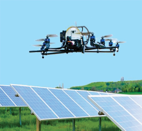
Drones equipped with infrared cameras can be used to inspect solar farms. Credit: TÜV Rheinland
‘The method [photoluminescence] can be used in all steps of the manufacturing chain to find electrical defects and process errors. Finished solar cells or modules can simply be excited via the contacts as an alternative to the laser. This method, called electroluminescence, is now offered at very low cost and is part of solar cell inspection or module control,’ he added.
Remote monitoring
According to Magnus Herz, senior expert, R&D at TÜV Rheinland, although optical methods of fault detection in photovoltaic power plants have been used in the photovoltaic industry for many years, uptake has been limited because it takes a lot of time and labour to make these measurements across a large solar plant comprehensively. As an alternative, he said the strategy of using remote aircraft equipped with infrared cameras can be a cost-effective and much less time-consuming option for fault diagnosis over these solar farms.
He points out that solar module inspection benefits from infrared and electroluminescence imaging techniques – both of which are widely used indoors and outdoors. ‘A combination of electroluminescence and infrared measurements was proposed to detect the most common defects in a solar module with high accuracy,’ he said.
‘Electroluminescence measurements take advantage of the radiative inter-band recombination of excited charge carriers in solar cells,’ he explained. ‘The solar cells are supplied with a defined external excitation current, while the camera takes an image of the emitted photons. Damaged areas of a solar module appear dark or radiate less than areas without defects. The high resolution of the electroluminescence images enables the resolution of some defects more precisely than in infrared images [alone].’
Image evaluation
Broadly speaking, the Fraunhofer ISE team views the hardware of its infrared devices as mature, and does not anticipate any further additional technical innovations in the near future. That said, Haunschild said there has been great progress in the area of image evaluation, particularly in photoluminescence imaging.
‘Measurement results contain a lot of information about the quality of the wafers and, since no one can look at all the high-resolution data in production, powerful image analysis based on machine learning and artificial intelligence is needed to extract the essential information from the images to make them usable for quality control and process development,’ he said.
‘As a concrete example, we have been working on quality control of kerfless wafers from NexWafe in particular over the last year,’ he continued. ‘This is a very exciting technology with many advantages over classical silicon.
‘The infrared reflection method could also be considered as still relatively new,’ he added. ‘It was developed in industry and has some advantages over classical infrared transmitted light.’
Meanwhile, although unaware of any major recent technological or operational breakthroughs in the use of infrared technologies for solar cell inspection, Grodzki pointed out that higher resolution, shortwave infrared cameras can be used for higher detail – and that near infrared-sensitive CCDs can also be used in some cases.
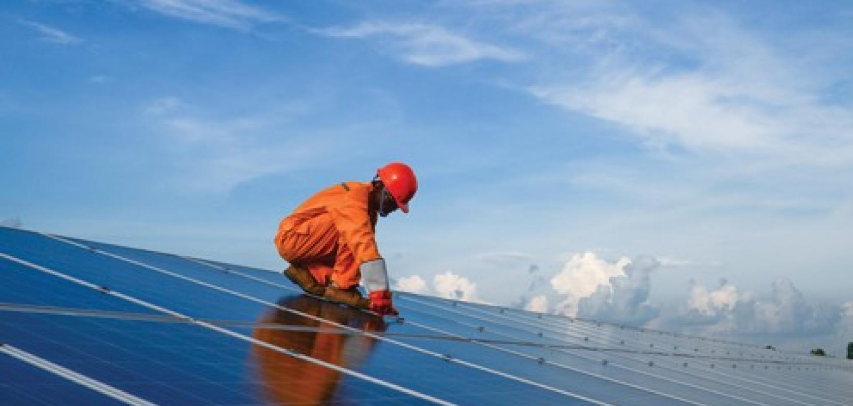
Solar panel inspection. Credit: Teledyne
He added that higher resolution and lower cost can be achieved with colloidal quantum dot SWIR sensors. ‘Although the quantum efficiency of these devices is somewhat lacking today, the technology is quite promising,’ he said.
Higher yields
When it comes to assessing the advantages of using infrared imaging, Grodzki pointed out that, although other techniques exist that enable users to detect defects on the surface of solar cells, only infrared can equip observers with more information about the material being used and the resulting outputs.
‘The use of infrared techniques results in higher yields for the manufacturer,’ he said. ‘Finding the right mix of infrared detector, illumination and optics can be a challenge, but many machine vision distributors have the knowledge to assist with this.
‘Another challenge for customers is price – higher sensitivity means a higher cost,’ he added.
Meanwhile, Haunschild observed that decisions relating to the application of these infrared imaging methods in industrial processes always entail detailed cost-benefit considerations, and depend on the relative value placed on internal quality control.
‘My personal impression is that a lot of emphasis is placed on this, especially in western countries, which is why infrared transmitted light or infrared reflection is widely used as part of the entrance test for microcrack control,’ he said.
Despite the undoubted benefits, Haunschild pointed out that photoluminescence imaging is quite expensive because a strong laser and a safe enclosure are needed – meaning it is mainly used in the laboratory and rarely on production lines.
‘If prices can be reduced and the technical concepts simplified, this could also change, [and] we [Fraunhofer ISE] are actively working on this. We consider the hardware concept to be mature… for demanding scientific applications. If one is willing to compromise in favour of price, the rapid developments in camera and LED technology over the last few years open up new possibilities that will hopefully result in simple and cost-effective photoluminescence measurement devices,’ he said.
Future developments
Looking ahead, Grodzki is hopeful that detectors will become more responsive over time, which would reduce the requirement for costly and powerful infrared illumination – a development he views as especially relevant for shortwave infrared.
‘Automated solar panel inspection will also be further enabled by the combination of drones and thermal imaging,’ he added.
Meanwhile, Haunschild predicted that the introduction of new solar cell concepts will inevitably bring new inspection requirements.
‘On the one hand, due to the boom of monocrystalline wafers, we see more and more specific defects, which are known from earlier years but had disappeared in the industrial environment. In particular, thermal donors can be a problem for heterojunction solar cell concepts. However, with appropriate hardware and the right image analysis, these defects can be evaluated and bad wafers can be detected,’ he said.
‘On the other hand, researchers are currently working feverishly to introduce tandem solar cells into the industrial environment,’ he added. ‘In principle, these are two solar cells [placed] on top of each other to capture and use even more light. This structure is only partially measurable with the established infrared systems and requires adjustments in the technology.’
Taking the heat out of solar
As Magnus Herz, senior expert, R&D at TÜV Rheinland, explained, one of the most important pieces of data captured by infrared images is the temperature difference between various parts of a solar cell module, or between modules or strings of modules.
‘Inactive areas of a module or string usually appear hotter than surrounding active areas. When a photovoltaic module or string is not functioning, the energy generated is not converted to DC power and remains as excess heat, raising the temperature of the module or string,’ he explained.
‘A great number of failures on photovoltaic modules can be detected using infrared imaging, from hot spots to mismatch losses or installation failures,’ he added.
Broadly speaking, there are two different types of infrared or thermographic cameras – those with cooled detectors and those with uncooled detectors.
The sensors used in cooled thermographic cameras are made from narrow band gap semiconductors. However, although such cameras possess very high sensitivity, they are not commonly used in photovoltaic applications because of the cost and complexity of the associated cooling system.
‘Commonly used thermographic cameras are based on uncooled sensors that can work at ambient temperatures. The most common sensor architecture is the microbolometer,’ Herz said.