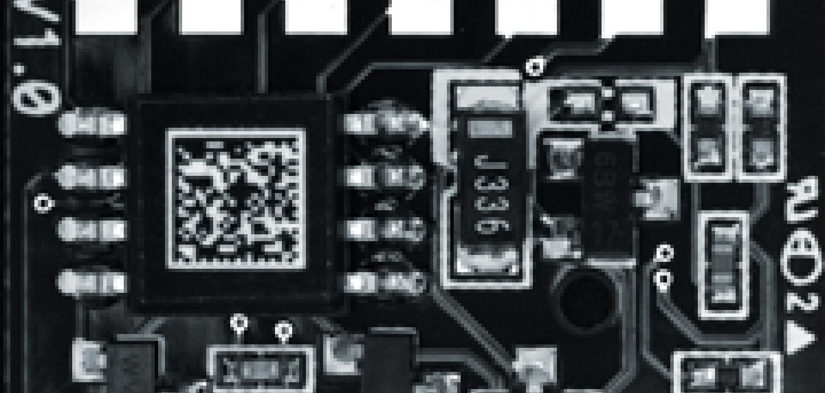
Within the realm of consumer electronics, size most definitely matters. Designers of electronic products – from smartphones to flat screen televisions to the latest video game consoles – are tasked with dramatically increasing the level of functionality of these devices while keeping them small and compact.
For manufacturers, the challenge is to ensure the huge volumes of electronic devices made are subject to a high level of scrutiny on the production line, so that every single one has been produced to the same exacting standards. To do otherwise would risk consumers losing faith in a brand that is undoubtedly already under fierce competition within a saturated marketplace. Manufacturers are therefore turning to the latest machine vision inspection systems.
‘All technologies in machine vision are being pushed to the limits in the realm of electronics inspection,’ commented Greg Hollows, director, Imaging Business Unit at Edmund Optics. ‘There are many photonics technologies that are now being used in the machine vision space to help solve the rapidly growing range of applications that the electronics industry is creating. Machine vision is being used to inspect nearly everything – from the printing on components to their placement and alignment in a device, to actually testing the screens and advanced features on those devices.’
The finer details
According to Johannes Hiltner, product manager for Halcon at MVTec Software, matching and positioning are the standard and therefore most important machine vision tools used in the electronics arena. These are used, for example, for board alignment or fiducial localisation, both of which are the most basic processing steps within electronic device production. He added that multi-camera setups are enabling high-precision 3D image processing, which is not only the natural progression from 2D technologies, but offers many additional advantages. For example, 3D technologies enable not only presence checks but also volume measurement, which comes in handy for high-precision solder paste inspection.
When it comes to board inspection and wafer inspection, MVTec’s Halcon and Merlic software solutions recognise defects with an accuracy greater than 1µm. From insufficient soldering paste to missing diodes and rotated components, the software detects all incomplete or incorrectly positioned parts within milliseconds. Moreover, it can find objects with an accuracy better than 1/20 pixel if they are partially occluded.
‘Component identification technologies, like barcodes, data codes and text recognition, should also be mentioned here,’ said Hiltner. ‘With this technology, manufacturers can ensure that the correct parts are being placed and assembled. Thus, each component can be traced through the whole production process. Advances such as high-resolution cameras, advanced computation technology and highly sophisticated algorithms enable high-speed processing, accuracy and robustness.’ Another important technology in the inspection process highlighted by Hiltner is sub-pixel accurate high-precision 2D measuring, which is used for presence checks of electronic components.
In terms of the technology being deployed, Edmund Optics’ Hollows noted that 3D metrology, spectroscopy, and hyperspectral imaging are all becoming part of electronics inspection. The two key elements that are making this possible are the growth of lower cost, more efficient sensors and lighting technologies. Furthermore, more powerful optical design software is allowing for advanced optical designs to meet needs associated with developments in sensor technology. There are also improvements being made in optical fabrication and metrology equipment for producing these designs.
Lenses play a critical role in electronics inspection, and the latest Techspec telecentric lenses from Edmund Optics are well suited to both single unit inspection stations and high volume implementations. The company has recently launched six new models with longer working distances of 220mm and 300mm into its Techspec compact range of telecentric lenses. These latest releases bring the model count within the range to 40, with magnifications varying from 0.5x to 8x and working distances from 40mm to 300mm. All sizes and working distances are available in models with an in-line illumination option, and are designed with a port to connect a fibre optic light guide or LED module. The fixed aperture and lockable focus of these lenses make them ideal for implementation on assembly lines as they remain permanently fixed.
On the factory floor
‘Due to the higher need of automation technology and the ongoing growth in consumer electronics production over the past decade, the factories in the [electronics] industry, of course, are demanding three important quality aspects in their production: high-speed processing, accuracy and robustness,’ said MVTec’s Hiltner. ‘This is why machine vision is playing a more and more important role within the [electronics] industry.’
‘In general, production processes are getting faster, and with technologies like 3D scene flow, robots and humans are working together hand-in-hand in order to realise a true Industry 4.0 environment and work atmosphere,’ continued Hiltner. Industry 4.0 stands for the fourth industrial revolution, which largely revolves around digital production and factory processes interconnected and automated via the internet. Electronics manufacturers like Siemens are leading the way in Industry 4.0 – its Amberg, Germany factory is a good example making 12 million Simatic PLCs a year.
‘Machine vision as “eye of the production” is one of the most important drivers of Industry 4.0,’ Hiltner added. ‘Thus, and because of its various fields of application, it will have a huge impact on the future of every factory as more and more production processes, even complex production steps, are being automated.’
Edmund Optics’ Hollows agreed that factories have the potential to become fully automated, removing the need for the current work force to engage in dull, dreary, and sometimes dangerous work.
As the level of automation rises, manufacturing costs reduce, but in order to meet demands – especially in terms of handling smaller parts and higher production speed – Hiltner said that the speed and accuracy of existing fundamental image processing technologies, like matching and measuring, need to be improved. Furthermore, the range of available technologies needs to be expanded with new efficient algorithms and methods, such as 3D measurement or 3D inspection.
There are, however, mixed issues when considering the emergence of inspection technologies within this field. ‘Many of these technologies are moving from laboratory-level use to factory-level use at a rapid pace, and the robustness of these technologies to hold up to the wear and tear of a factory floor environment is a significant challenge,’ Hollows explained. ‘Just the shipment and set-up of some technologies can be a problem, let alone dealing with rapid temperature and humidity changes, high levels of vibration, and the dirt and dust that can be produced. Usually, these issues do not mix well with precision optical- and photonics-based equipment.’
He added that another issue is the incredibly fast-paced development environment. Because of the competitive nature of the electronics market, some applications go from concept to deployment before true validation can be carried out.
While demand for this technology remains high and diverse, in Hollows opinion there will be a bit of a lull in the market’s growth because of consumer exhaustion from new technology in the phone, tablet, and display space. ‘This is normal in a mostly saturated market; however, the next big things are not that far away,’ he said. ‘VGR (vision guided robotics), virtual or augmented reality, and autonomous vehicles all hold promise for driving the development curve for machine vision forward at an accelerated pace.’
Hollows remarked that the machine vision industry needs to be willing to take the same risks as the electronics sector. ‘You have to develop new products and technologies before the volume demands really exist,’ he concluded.