Imaging and Machine Vision Europe talks to previous honoree of The Photonics100 Jan Bogaerts, CTO of Gpixel, a company that supplies advanced CMOS image sensors.
What is the next big thing in your area of photonics research?
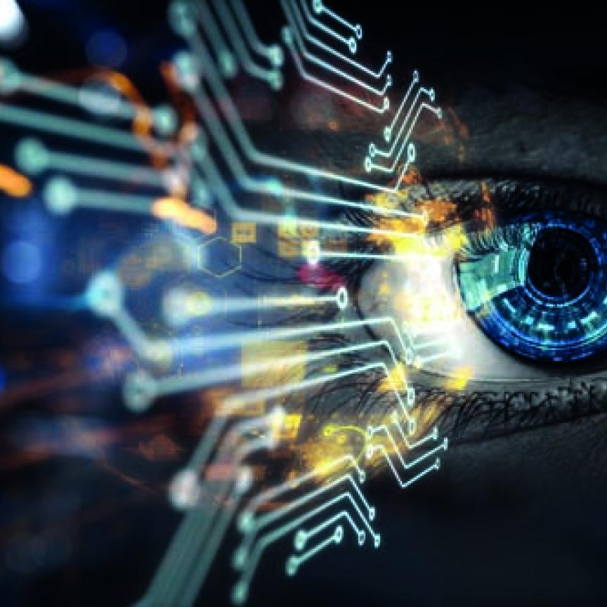
I’ve been working on the development of image sensors during my whole career. What's struck me is that they’re being used in an ever-increasing variety of applications, with a continuing push for the best compromise between performance, speed, and cost.
This results in very different types of sensors for mobile phones, industrial vision, medical applications, scientific and space applications, and more. We’re able to develop new and better-performing sensors since we can rely on the worldwide push for technological advancements in the semiconductor industry, not only for CIS technologies but also in other and larger markets for processors, memory, and so on. One example of such a technological breakthrough is the 3D stacking of two or more wafers.
What do you think the biggest challenges in your area will be over the next year?
When developing sensors, we need to find the best trade-off to achieve certain features, using available technologies or process advancements during development, and within a given project budget and time schedule. Since 3D stacking brings new degrees of freedom into the design, it creates opportunities for additional features, increased on-chip processing and bandwidth, and more. However, it also makes the sensor architecture and design process more complex, and thus brings challenges in terms of balancing all these parameters while keeping realistic project schedules. On the other side, we have seen important advancements in recent years in low light imaging and photon counting, 3D and lidar, extensions of the wavelength range and high dynamic range, and more.
What is the biggest personal challenge you have overcome?
Technology is advancing very quickly, which can be overwhelming and sometimes inaccessible at first. It’s always good to think about design and technological risks and uncertainties. There will always be reasons to use existing solutions, but when possible and needed, one should dare to push beyond the state-of-the-art, leave the comfort zone and think about the longer-term targets.
What advice would you give to someone embarking on a career in photonics research?
Think about your best skills and motivations, then think about the best place to employ these skills, and learn to develop in other areas. And since no one is able to conduct advanced research on their own, it’s of utmost importance to become part of a team that’s experienced and ambitious in its targets, while at the same time welcoming junior people to grow and learn from delays, mistakes, and so on. Nothing is more satisfying than succeeding in pushing the technological boundaries within an environment where a lot of different skills are required and where there is a great team spirit and culture to push and mentor each other.
Who has been the biggest help to you in your career?
It’s very hard to name a single person. I’ve had the luck to work with many people that challenged my ideas or proposed approaches, but at the same time trusted me to achieve certain minimum requirements. It’s from those cases where you take unknown routes that you learn most, even when not always fully achieving the ultimate performance you had hoped for.
You can make your nomination for The Photonics100 2024 here.