Sony has released two SWIR sensors, boasting 5μm pixels and the ability to image across both the visible and short-wave infrared. Edmund Optics’s Thomas Armspach-Young and Boris Lange consider the optics needed to get the best out of these sensors
Short-wave infrared (SWIR) imaging has been gaining traction over the last few years. Significant progress has been made in SWIR cameras and sensors, which has reduced integration complexity and cost, and allowed the technology to enter more application spaces. Machine vision, process monitoring, medical, as well as safety and security are just a few examples.
One of the notable events on the horizon will be the launch of two new Sony sensors covering the visible and SWIR wavelength range simultaneously. This article looks at SWIR imaging from an optics perspective.
What is SWIR?
While not strictly defined, the SWIR range lies approximately between 0.9µm and 1.7µm, just beyond the part of the electromagnetic spectrum that is visible to the human eye. Thus, SWIR light can reveal details that are invisible to the naked eye, effectively enabling the user to see beyond the visible.
SWIR wavelengths behave similarly to those in the visible range, where photons are either transmitted, reflected or absorbed by an object, as opposed to mid-wave infrared (MWIR) and long-wave infrared (LWIR) radiation which is emitted from the object itself.
This property of SWIR allows for a crisper image with higher resolution and stronger contrast – both critical criteria for machine vision applications – when compared to the more blurry images produced by thermal emissivity using MWIR or LWIR wavelength bands.
However, there are substantial implications when comparing SWIR to visible imaging. On the camera side, the quantum efficiency of silicon is zero, which makes visible sensors unusable for SWIR applications – InGaAs sensors are used instead.
Optical design
As with the sensor technology, moving from visible to SWIR has implications on the choice of imaging lens. Fairly large pixel sizes of around 15µm to 30µm, which are common among InGaAs sensors, make it easier to meet optical resolution requirements. The large pixel size is also the reason why sensor sizes, even at VGA resolutions (640 x 480 pixels), tend to be larger compared to what is most commonly used in visible sensors.
When going polychromatic in SWIR or if high transmission is needed, the number of optical glasses available to the designer is significantly reduced, as most glasses used in the visible region start to show absorption in SWIR. In addition, when it comes to colour aberrations, SWIR is a difficult waveband for optical designers to correct for as the glasses behave very differently when compared to how they interact with visible light. With increasing wavelength, the flints (high dispersion glasses) start to act like crowns (low dispersion), which makes it tricky to design an achromatic solution using commercial optical glass because of the lack of difference in their dispersion. This drives up costs substantially, as those speciality glasses are not produced in volume and are not easy to machine.
A more exotic option would be to use a lens design that uses infrared crystalline materials (ZnSe, ZnS, Ge, CaF2) as a substitute for high dispersion glasses. While being a more compact and lightweight solution than the former, the addition of these infrared materials will significantly increase the cost of the lens assembly. Furthermore, infrared crystals tend to have poor thermo-mechanical properties and are typically more susceptible to chips and scratches during the manufacturing process or when exposed to harsh environments. As a consequence, most if not all off-the-shelf lenses today are based on spherical glass elements.
For coatings, it is possible to design a broadband coating covering the 0.9-1.7µm waveband without too much difficulty. However, if a high-performance anti-reflective coating were to be designed to cover visible and SWIR regions there would most likely be a considerable increase in cost, as well as there being potential angular sensitivity issues caused by the multiple coating layers that would be required.
The new Sony IMX990/991 sensors are expanding the usable waveband to allow for imaging both visible and SWIR on the same sensor. Reducing the pixel size to 5µm adds to the complexity, but the comparably small sensor sizes of ¼-inch or ½-inch (~8mm diagonal) will reduce some of the issues that designers face. Overall, it will still be challenging for optics manufacturers to design off-the-shelf products for this sensor.
Performance of Edmund Optics' SWIR 50mm lens across VIS-SWIR range
The plots in figure one highlight a few of the challenges when designing a lens over such a wide waveband. The Edmund Optics 50mm FL SWIR lens (#83-165) was used to generate the data. First, the chromatic focal shift curve (CFS) shows how the plane of best focus (x-axis) varies for different wavelengths (y-axis). At 0.4µm, one can see that the plane of best focus starts far out at 300µm. However, between 0.5µm and 1.7µm, the curve – the plane of best focus – stays within a comparably small range of 90µm, crossing the zero position of the x-axis twice at ~0.5µm and 0.9µm. One can also extrapolate that the curve will pass the zero position of the x-axis a third time for a wavelength greater than 1.7µm. This behaviour is referred to as apochromatic. It is worth pointing out that most off-the-shelf lenses will only show an achromatic behaviour, meaning the CFS curve will have a parabolic shape and pass the plane of best focus only twice. Consequently, the longitudinal chromatic aberrations will be much more pronounced, limiting image quality.
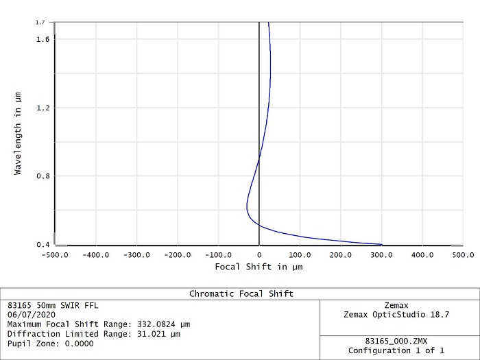
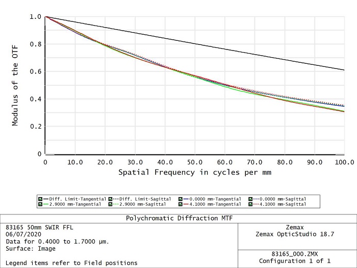
Figure 1: Chromatic focal shift (top) and nominal modulation transfer function (bottom) plotted at 750mm WD, f/2.8, 0.4 to 1.7µm wavelength range in 0.1µm steps, equally weighted
Despite the large amount of chromatic focal shift (330µm) over the entire waveband, the nominal modulation transfer function (MTF) curve indicates a very good performance of 30 per cent contrast at 100lp/mm over the entire ½-inch sensor. The long focal length of the lens combined with the comparably small sensor size is very beneficial in that context. It should be noted that manufacturing tolerances will lead to a reduced MTF performance compared to the MTF curve shown here. Nevertheless, the nominal starting point of 30 per cent contrast is quite promising
Applications
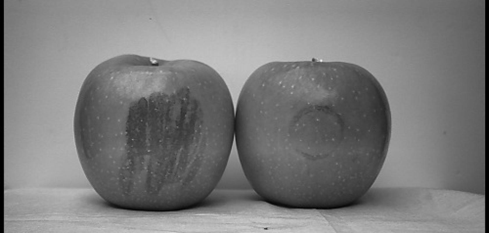
SWIR imaging is successfully used in a number of applications. It exceeds the capabilities offered by visible imaging as different materials absorb and transmit SWIR wavelengths differently. Examples of how absorption is used to create contrast can be found in food inspection where a specific SWIR waveband is strongly absorbed by water – bruising in fruit, for instance, will have a higher water content than the surrounding tissue and therefore show up clearly with a SWIR camera.
Sugar, salt and starch can also be distinguished according to how they absorb SWIR light. In order to choose the ideal waveband that maximises contrast, the absorption spectra of the materials at hand have to be determined.
The second approach to create contrast is based on differences in transmission, such as viewing a scene through fog, which a SWIR camera is able to do, whereas a visible camera would struggle.
Outlook
As advances on the camera and sensor side continue, SWIR technology will also continue to be deployed both in existing as well as new applications, from defence and security markets (day/night vision, range detection, surveillance) to commercial markets (non-destructive testing, industrial process monitoring, autonomous vehicles).
The SWIR market is expected to grow considerably over the next few years where this demand is driving sensor manufacturers to create smaller and more cost-effective solutions.
Sony’s IMX990/991 sensors provide a unique addition to the SWIR imaging market, and the technology has great potential in many applications. Designing optics for these sensors will be challenging, yet it will be interesting to see what kind of products will be launched in this field as time goes by.
The authors
Thomas Armspach-Young (ThomasA@edmundoptics.co.uk) is an applications engineer for imaging and machine vision at Edmund Optics, while Boris Lange (BLange@edmundoptics.de) is manager imaging Europe at the firm.
--
Sony's SWIR sensors
Sony's IMX990 is a 1/2-type sensor (8.2mm diagonal image size) with 1.34 megapixel resolution; the IMX991 sensor is a 1/4-type (4.1mm diagonal) with 0.34 megapixel resolution.
The new products employ Sony's SenSWIR technology, in which photodiodes are formed on an InGaAs layer and are connected via copper-to-copper bonding with the silicon readout circuit layer.
Traditional SWIR image sensors, made using indium bumping to bond the InGaAs layer to the silicon layer, face manufacturing challenges to shrink the size of the pixels and increase pixel count. It is necessary to secure a certain bump pitch, which makes it difficult to achieve a smaller pixel size compared to current industrial CMOS sensors.
There are other issues with conventional SWIR sensors, including low sensitivity in the visible light spectrum. These factors have inhibited the penetration of SWIR imaging.
Sony's new sensors, based on the company's stacking technology using a copper-to-copper connection, means a 5μm pixel size can be achieved. This gives a high image quality and a more compact sensor size.
The technology is also used to make the top InP layer – which absorbs visible light – thinner, making it possible to transmit light to the InGaAs layer underneath. This means the sensor has high quantum efficiency even in the visible range.
The new products also support digital output, matching the performance of current CMOS image sensors for industrial equipment.
IMX990
- Pixels: 1296 (H) × 1032 (V), approx. 1.34 megapixels
- Image size: diagonal 8.2mm (1/2-type)
- Unit cell size: 5μm (H) × 5μm (V)
- Frame rate – full pixel: 8-bit: 130 fps; 10-bit: 120 fps; 12-bit: 70 fps
- Power supply: 2.2 V, 1.2 V (pixel); 3.3 V, 2.2 V (analog); 1.2 V (digital); 1.8 V (interface)
- Main functions: Global shutter, digital thermometer, ROI
- Output: SLVS (2/4ch switching)
- Package: Ceramic PGA with built-in thermoelectric cooling; 30.0mm (H) × 30.0mm (V); Ceramic LGA: 20.0mm (H) × 16.8mm (V)
IMX991
- Pixels: 656 (H) × 520 (V), approx. 0.34 megapixels
- Image size: diagonal 4.1mm (1/4-type)
- Unit cell size: 5μm (H) × 5μm (V)
- Frame rate – full pixel: 8-bit: 250 fps; 10-bit: 240 fps; 12-bit: 130 fps
- Power supply: 2.2 V, 1.2 V (pixel); 3.3 V, 2.2 V (analog); 1.2 V (digital); 1.8 V (interface)
- Main functions: Global shutter, digital thermometer, ROI
- Output: SLVS (2/4ch switching)
- Package: Ceramic PGA with built-in thermoelectric cooling; 30.0mm (H) × 30.0mm (V); Ceramic LGA: 20.0mm (H) × 16.8mm (V)