Camera systems measuring millimetres and costing only one dollar are now possible thanks to electronic and optical developments in wafer-level technology.
Antonio Gomes of semiconductor manufacturer Ams spoke about manufacturing minature cameras at the EMVA’s debut Embedded Vision Europe conference in Stuttgart from 12 to 13 October.

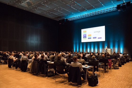
The first Embedded Vision Europe Conference attracted around 200 participants. (Credit: EMVA)
Gomes remarked that digital camera module heads measuring 0.7 x 0.7 x 1.1mm have already been produced for medical endoscopy - when Ams acquired Cmosis in 2015, it also acquired technology from Awaiba, which developed sub-millimetre CMOS modules for endoscopes. Gomes added that by introducing additional electronics to the system, fully functioning cameras can be produced, and can be done so for less than one dollar.
‘It’s known that visions systems are expensive, bulky, and consume a lot of power, so that’s something we want to change,’ Gomes said. ‘Nowadays cameras really don’t need to be bulky... In the past five years I’ve been helping customers to drive vision into the smallest places that you can imagine.’
In order to compress the vision technology into millimetre volumes, Ams has had to reduce the chip size of the system, optimise power consumption, select a suitable interface, use wafer-level lens technology, and shrink the size of the camera housing.
For the chip, a considerable contributing factor to its size is the pixel area, as this has to be fixed depending on the resolution. Ams therefore had to focus on reducing the size of the surrounding area – the periphery – and was able to bring this down to 85μm. The chip still included vital components and functionality, such as the pixel guard ring; edge of die, row and column; analogue-to-digital convertors (ADCs); a serialiser; an LVDS driver; power-on reset; and four contacts for through silicon vias on the backside.
To improve the power consumption Ams has optimised the ADCs and off-chip driver architectures; they measure 0.08mm2 and consume 0.36mW of power. The LVDS driver architectures were also optimised to use only the minimal current necessary.
When considering the most suitable interface to use, LVDS, MIPI, CIF, I2C and SPI were all candidates that were either too power hungry or took up too much space in the system. Ams is hoping to overcome this by implementing MIPI I3C in its next generation of devices, which offers both low power consumption and low volume while being able to drive a complete data stream.
Miniature optics are also essential for such a small camera. Modern wafer-level technology now allows multi-element micro-lenses to be packaged into a stack and bonded to the chip of the camera.
Three main technologies are available for producing wafer-level optics, according to Gomes: plasma etching, which requires long processing times and presents limitations in lens height; glass formed lenses, which are no longer used because of process stability issues; and UV replicated polymer lenses. It wasn’t disclosed by Gomes which technology was used by Ams in producing its cameras.
‘Current technology allows us to make multiple types of lenses at wafer-level, such as twin lenses, dual lenses, hybrid lenses and Fresnel lenses,’ said Gomes. ‘Multiple lenses can be combined together in the same model.’ Ams recently acquired Heptagon, a firm with expertise in replicating optics in wafer-level packaging, which can now be used by its new owner to house the wafer-level optics in the camera. Wafer-level chip-scale packaging offers both size and cost benefits over traditional wire bonded assemblies thanks to its simpler assembly process, according to Gomes.
Ams’s upcoming NanEye camera module is a full camera system using multiple element wafer-level lenses in a footprint of around 1 x 1mm. The pixel array has a size of 750 x 750μm and enables resolutions of 250 x 250 pixels (using 3µm pixels) or 320 x 320 pixels (2.4µm pixels), with 500 x 500 pixels (1.4µm pixels) also being introduced in 2018, according to Gomes. He said that while the resolutions are not as high as other vision systems, they are adequate for applications such as endoscopy, gesture recognition, and eye tracking. The micro-cameras can also be used in multi-camera solutions to provide features such as stereovision, allowing 3D measurements to be taken in confined spaces.
Increasing the resolution of wafer-level optics is particularly challenging, Gomes pointed out, as the lenses themselves don’t necessarily have high enough resolving power to be able to take advantage of the higher pixel count.
The size of the micro-cameras means they can be fabricated in large volumes and for very little cost. According to Gomes, a 300mm image sensor wafer can be used to produce 66,000 1 x 1mm devices at a cost of 20 cents each, and a 100 x 100mm glass substrate can be used to produce 6,000 1mm-size lenses. When combined to form a full, high-performance camera system, the cost rises to just under one dollar per camera. This low cost makes the cameras perfect for disposable applications, particularly in medicine.
Ams believes that thanks to their low cost and their ability to be produced in large numbers, the micro-cameras will enable a wider uptake of vision to take place as anyone will be able to afford them.
‘We believe the use of cameras for automated vision will become ubiquitous,’ Gomes concluded.
Related article:
Deep learning for embedded vision highlighted at EMVA conference

