Greg Blackman finds that purchasing IP cores for FPGAs is one way to reduce time-to-market for camera production
Camera manufacturers are making more products with processing built in, thanks to the availability of powerful system-on-chips or other processor architectures. To ease the development effort of designing camera-host interfaces, firms including Euresys, Pleora, Kaya Instruments, and Framos now offer transport layer interfaces in the form of intellectual property (IP) cores that are ready to incorporate into field programmable gate arrays (FPGAs).
An IP core is a reusable block of logic that acts as a building block within FPGA or ASIC design. It shortens time-to-market and improves performance of vision development on FPGAs. CoaXPress, GigE Vision and USB3 Vision IP cores, for example, from Sensor to Image (S2I), part of Euresys, lower the engineering cost required to design the transport layer interface for these standards.
S2I has recently introduced an IMX Pregius IP core, providing an interface to Sony Pregius sub-LVDS image sensors. The company will also soon release an interface to MIPI sensors primarily used in embedded vision systems and mobile devices.
Korean camera manufacturers Ozray and Crevis, along with German firm Sick, have implemented S2I IP cores in their cameras. In testimonials collected by Euresys, Keith Ahn, executive director and CTO of Ozray, said that in-house development of CoaXPress and GigE transport layer interfaces would have been considerably more expensive than purchasing IP. June Hwang, CEO of Crevis, said that in the past it took a considerable amount of engineering manpower to develop the internal transmission logic, device drivers and Tx/Rx library for transport layer interfaces for its area scan cameras. Hwang added that by purchasing the IP cores, its engineers can focus on developing the sensor interface and camera functionality.
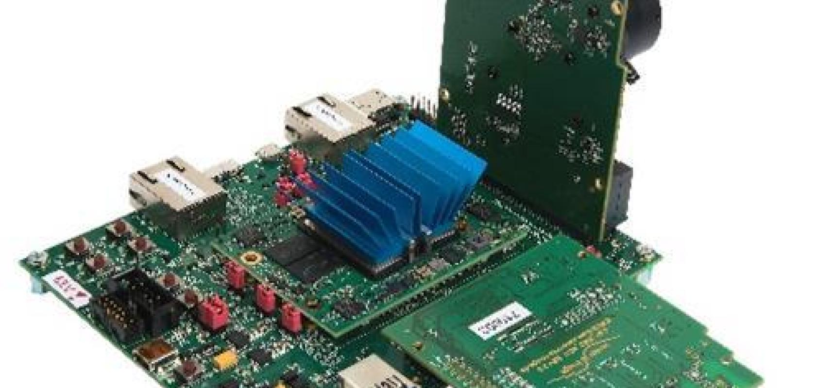
S2I’s Vision Standard IP cores (CoaXPress, GigE Vision and USB3 Vision) are delivered as a working reference design along with FPGA IP cores that have been tested against a wide range of frame grabbers and image acquisition libraries. They are compatible with Xilinx 7 series FPGAs and newer models, and Intel/Altera Cyclone V and more recent devices.
The top-level design, consisting of the interface between the image sensor and transport layer PHY, is delivered as VHDL source code. The video acquisition module of the reference design simulates a camera with a test pattern generator. This module is delivered as VHDL source code which is replaced by a sensor interface and pixel processing logic in the camera design. An FPGA-integrated CPU – MicroBlaze, NIOS or Arm – is used for several non-time-critical control and configuration tasks on the Vision Standard IP cores. The software is written in C and can be extended by the customer.
Framos has developed its SLVS-EC RX IP core to reduce overhead and complexity when implementing a Sony image sensor with SLVS-EC interface. The IP core is an on-chip function block connecting the customer’s FPGA logic with the image sensor’s data stream. It receives the interface data and manages the byte-to-pixel conversion for various lane configurations.
Kaya Instruments offers a CoaXPress 2.0 IP core, while Pleora’s CoreGev-Tx10 GigE Vision FPGA IP core supports up to 10Gb/s transmission of uncompressed images over a standard Ethernet connection.
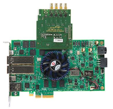
Intel Cyclone 10 evaluation board with CXP interface board. Credit: Euresys
Xilinx has also developed time-sensitive networking IP cores with some of it partners, which one day could be used in machine vision cameras, according to Chetan Khona, Xilinx’s director of industrial, vision, healthcare and sciences. Khona was speaking to Imaging and Machine Vision Europe in the run-up to the SPS show at the end of November in Nuremberg, Germany.
Some of the Xilinx’s machine vision customers have already purchased its IP core for TSN, Khona said, and are integrating it as a way to get their cameras connected on future industrial networks, TSN as the back layer with OPC UA as the application layer.
Time-sensitive networking supports multiple classes of traffic over one network. A network is homogenous and all the data is treated equally in classic Ethernet, but in TSN different data streams can be assigned classes and given different levels of priority.
‘We’ve had machine vision customers purchase our IP cores and get ready for this dawn of OPC UA,’ Khona said. At SPS, many exhibitors will be advertising the fact that their products support Industry 4.0 or OPC UA.
Xilinx’s Zynq system-on-chips are a popular processor among machine vision camera manufacturers, and Khona expects machine vision to transition further from the ‘dumb’ camera into smart or embedded cameras.
One of the reasons for this transition is that it’s easier to bring processing to data than it is to bring data to the processing. Traditionally, in machine vision systems, this hasn’t held true – sensor data is taken by a frame grabber and processed on a PC. But with smart cameras more processing is done in the camera rather than shipping it off elsewhere. IP cores offer a faster way to develop smart cameras based on FPGAs.
Are you using FPGAs?
If you would like to write about your experience developing and deploying an imaging system using FPGAs, please get in touch: greg.blackman@europascience.com