Direct communication between FPGAs and GPUs
Philipp Huber, Hans-Joachim Gelke and Matthias Rosenthal, from the Institute of Embedded Systems at Zurich University of Applied Sciences, describe a method for direct data transfer between a GPU and FPGA for real-time imaging
GPUs with their immense parallelisation are best fitted for real-time video and signal processing. However, in a real-time system, the direct high-speed interface to the signal sources, such as cameras or sensors, is often missing. For this task, field programmable gate arrays (FPGAs) are ideal for capturing and preprocessing multiple video streams or high-speed sensor data in real time.
Besides the partitioning of computational tasks between GPU and FPGA the direct communication between GPU and FPGA is the key challenge in such a design. However, since the data communication is typically controlled by the CPU, this often becomes the bottleneck of the system.
In an implementation based on the Xilinx XDMA IP, for example, the host can initialise any direct memory access (DMA) transfer between the FPGA internal address space and the I/O-memory address space. This allows direct transfer between the FPGA internal address space and the mapped GPU RAM. However, the host has to initialise each data transfer. As a result, an application has to run on the host, which is listening to messages from the devices. This application starts the data transfer if the devices are ready.
At the Institute of Embedded Systems, an entity of Zurich University of Applied Sciences, we’ve developed a new method for an efficient GPU-FPGA co-design called frame-based DMA (FDMA). This is based on GPUDirect, supported by Nvidia Quadro and Tesla GPUs, but without using the CPU for data transfer - it’s direct data transfer between the FPGA and the GPU. This versatile solution can be used for a variety of different applications, where hard real-time capabilities are required.
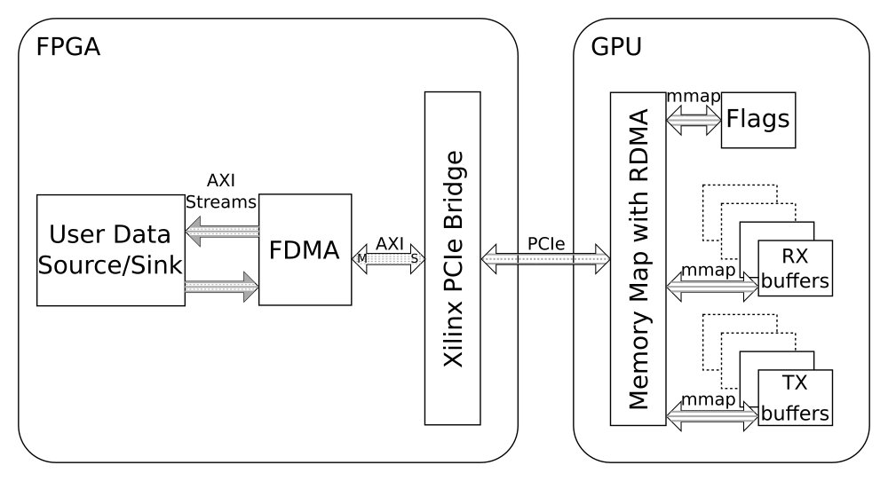
Frame based DMA implementation
The institute’s FDMA is designed to work without any host interactions after system setup. This approach uses the AXI to PCIe Bridge IP from Xilinx to translate AXI transactions to PCIe transactions. FDMA supports multiple RX and TX buffers in the GPU. This means one buffer can be used for reading or writing, and the other buffers for GPU processing. Each GPU buffer has a flag in the GPU RAM. This flag indicates who has access to this buffer and is used for synchronisation between the GPU and the FPGA.
Data rate measurements were made using a Xilinx Kintex 7 FPGA with PCIe Gen2x4 and an Nvidia Quadro P2000 PCIe Gen3x16. The slowest link between them is PCIe Gen2x4 with a link speed of 16Gb/s. The team found that FDMA is faster for small transfers, because the host doesn’t have to initialise every transfer. For larger block sizes the Xilinx XDMA IP implementation is faster, because of performance issues in the Xilinx AXI to PCIe Bridge IP.
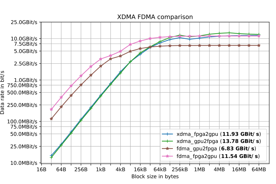
Average data rates comparing FDMA with XDMA
For real-time data processing a low execution jitter is needed. This execution jitter was measured with both implementations by measuring the transfer rate of 10 million data transfers of 32 bytes. The team found that the XDMA implementation has a huge transaction jitter. This is the case because the Linux host has to initialise every single transfer and Linux is not a real-time operating system. The two measurements of the FDMA implementation reveal that there is still a small transaction jitter when the X11 server is running on the same GPU, but it disappears nearly completely when disabling the X11 server.
In conclusion, both implementations, FDMA and XDMA make use of the direct transfer between the FPGA and the GPU and therefore reduce the load on the CPU. The FDMA developed at the Institute of Embedded Systems does not need any host interaction after setup and as such transfer jitter is extremely low. This makes the FDMA implementation perfect for time-critical streaming applications.
This white paper was taken from the Institute of Embedded Systems’ blog.
Further reading
Lowering development effort with IP cores - Greg Blackman finds that purchasing IP cores for FPGAs is one way to reduce time-to-market for camera production