At Photonics West 2015, held in San Francisco, USA, Imec released a new set of hyperspectral CMOS image sensors. The sensors feature spectral filter structures that are processed at wafer level which enables the sensors to be mass produced, opening them to multiple applications such as machine vision and consumer electronic devices.
‘Imec’s latest achievements in hyperspectral imaging emphasise how our promising technology has become an industrially viable solution for a number of applications,’ said Andy Lambrechts, programme manager at Imec.
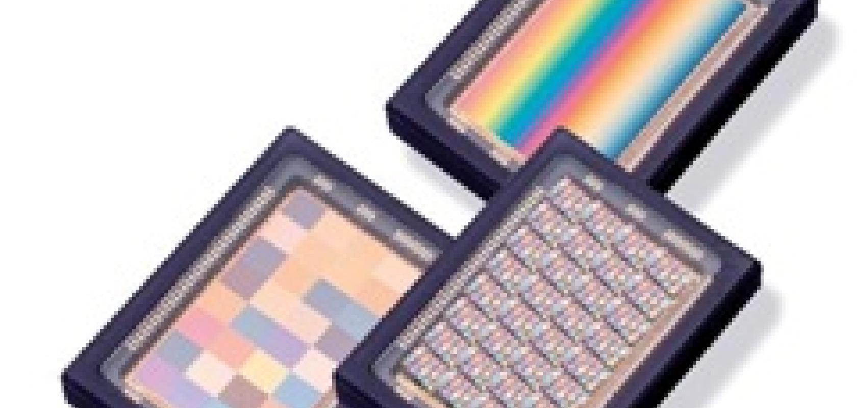
The spectral filters are laid out in a mosaic pattern on commercially available CMOS image sensor wafers. They are processed per-pixel on 4x4 and 5x5 Bayer-like arrays. Lambrechts said: ‘The new mosaic architecture, and extended spectral range, brings unique advantages compared to our previously announced hyperspectral linescan sensors for applications in which scanning would not be practical. It enables spectral imaging in a truly compact, tiny form-factor, that can even be scaled to handheld devices.
'From the technology standpoint, we have now successfully demonstrated linescan and tiled sensors, in which spectral filters cover many pixels, to mosaic sensors, in which filters vary from pixel to pixel. At the same time, the spectral range is extended and now covers down to 470nm.'
Imec demonstrated three different versions of these hyperspectral image sensors at Photonics West. The company also said first engineering samples have been manufactured and now available for evaluation to early partners.
Related links:
Click here for all of the latest CMOS news and products
Photonics West coverage from Electro Optics
External links:
