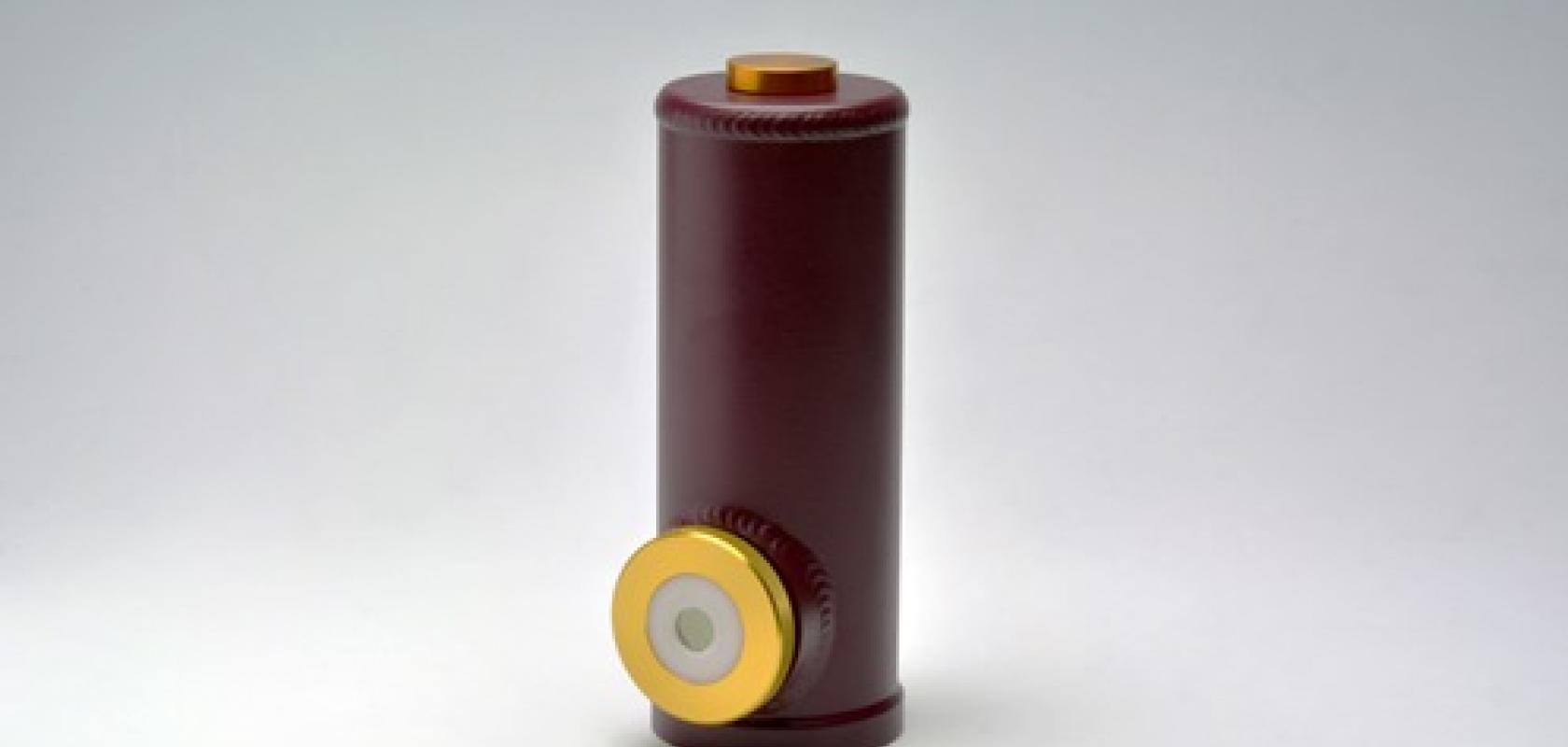
Hamamatsu Photonics has mass-produced a mid-infrared detector that doesn’t use hazardous substances restricted under the European Commission’s RoHS directive.
The compound opto-semiconductor is made up of 2,000 thin-film layers of InAs and GaSb, alternately laminated onto a substrate.
The detector is able to sense mid-infrared light at a wavelength of 14.3μm without using mercury and cadmium, common materials used for mid-infrared detectors but which are now restricted substances under the RoHS directive.
Hamamatsu said its new product will be ideal for analytical instruments such as FT-IR spectrophotometers, which rely on mid-infrared light to identify substances contained in the air, foods, and drugs. The new product can also replace existing mid-infrared detectors commonly used in gas component analysers and infrared thermometers.
Opto-semiconductors made of silicon are widely used for detecting visible light. Compound opto-semiconductors composed of two or more semiconductor materials are used to detect mid-infrared light with wavelengths longer than the visible light range. However, these compound opto-semiconductor structures are difficult to mass-produce.
Hamamatsu claims it is the first company to mass produce this type-II superlattice infrared detector. Its manufacturing technology is able to alternately laminate InAs and GaSb thin films with uniform thickness and high repeatability.