Industrial web inspection systems enable the improvement of manufacturing efficiency and product quality by helping to detect, minimise and eliminate defects and process errors.
Such systems are increasingly being automated, enabling manufacturers to more easily react to defects as they occur in real time.
According to the authors of ‘Application of automation for in-line quality inspection, a zero-defect manufacturing approach’, recently published in the Journal of Manufacturing Systems, poor product quality can increase firms’ financial losses, environmental impact, and waste of resources.
Poor quality can also have a negative social impact, affecting the reputation of a company through its substandard products and unsatisfied clients.
The authors of the research show that sustainable manufacturing can be achieved through the implementation of zero-defect manufacturing. “Making things right on the first try is the central tenet of zero-defect manufacturing,” they say. “In doing so, quality is enhanced and sustainability is raised, which ultimately results in higher customer satisfaction, which is crucial for a manufacturing company’s success.”
Through new system launches and industry case studies, Imaging and Machine Vision Europe recently learnt from vision firms how the automation of web inspection is bringing manufacturers closer to achieving the ultimate goal of zero-defect manufacturing.
New print inspection systems respond to quality demands
One of the main requests and imminent pressures from manufacturers when requesting web inspection technology is around quality, especially when their business serves high-end clients. “Customers’ demands on quality have risen continuously, especially for highly refined materials, brand owners, and luxury packaging,” says Dr André Schwarz, Marketing and Documentation Director at inspection system firm EyeC. “But, ‘normal’ fast-moving consumer goods (FMCG) packaging in the customer sector has also become increasingly high-quality. No compromises can be made, especially for customers working for companies in regulated industries – 100% quality and flawless products are essential.”
Staying on top of the game in order to meet the ever-growing demands of manufacturers requires a combination of integrated intelligence and innovative technology, meaning continuous R&D updates and launching the best products to meet customers’ expectations.
EyeC’s ProofRunner Wide Web system uses an 8k colour line scan camera to deliver ultrafast and precise 100% real-time print inspection in wide web applications ranging from 900-1,700mm
In response to customer demands, EyeC has recently launched a new web print inspection system, the EyeC ProofRunner Wide Web. Using an 8k colour line scan camera, the system offers ultrafast and precise 100% real-time print inspection in wide web applications ranging from 900-1,700mm. It compares the print image with a print-ready PDF file and automatically inspects texts, graphics, colour deviations, variable data as well as 1D and 2D codes reliably, providing documentation on the results.
The smart technology embedded in the ProofRunner Wide Web for labels, leaflets, and flexible packaging automatically detects defective areas, warning the operator in real time in the event of significant deviations. “With ProofRunner Wide Web’s real-time error detection, the operator at the press can immediately detect deviations from the artwork during the printing process, thus avoiding overproduction and misprints,” says Schwarz. Errors that can be identified immediately save expensive consumables and valuable machine time. “Our system prevents entire rolls from being produced incorrectly and directly helps the customer to produce more resource-efficiently and sustainably.”
Bettering battery inspection
Improving defect detection is crucial even in the most demanding applications, such as battery manufacturing – which, due to the rapid electrification of the mobility sector, is increasing rapidly – as noted by imaging firm Teledyne Dalsa’s Senior Product Manager Xing-Fei He.
He explains that in battery manufacturing, there are certain material types that require special inspection: “Anode (e.g. carbon) and cathode (lithium metal oxide) are coated on metal foils separately. These coated films are important parts of the battery cells and need to be inspected for thickness and related defects before moving into the next steps.” Defects such as thickness variation, blowholes, and particle contamination all need to be identified and prevented to ensure good yield, high product quality and safety.
Responding to such demands, Teledyne Dalsa recently launched AxCIS, a new family of high-speed and high-resolution fully integrated line scan imaging modules. These contact image sensors (CIS) combine sensors, lenses, and lights. This all-in-one combination offers a lower-cost inspection system for many demanding machine vision applications – including battery inspection.
Teledyne Dalsa recently launched AxCIS, a new family of high-speed, high-resolution fully integrated line scan imaging modules suited for web inspection
“AxCIS offers a fully integrated, easy-to-use, cost-effective line scan imaging solution to meet the requirements of space-limited systems, such as print, printed circuit board, and web inspection,” explains Xing-Fei. The new systems are powered by Teledyne’s new quadrilinear CMOS image sensor technology, which delivers up to 120kHz line rates for mono and 60kHz x 3 for colour, at 900 dpi resolution. This enables errors to be detected with exceptional precision, contributing towards the zero-defect manufacturing strategy.
Xing-Fei says AxCIS is targeting the increasing demands being placed on vision technology for automatic inspection with improved detectability, particularly in battery manufacturing. Through its 900 dpi high-resolution and HDR mode, the system is well positioned to deliver high-accuracy inspection of anode and cathode coatings.
Powering up paper production
Also striving for a future of automated, zero-defect manufacturing are vision firms Matrox Imaging and Active Inspection (AI), which through a case study share how one of AI’s web inspection systems can enable 100% inspection of surfaces, printing, and labels. The system includes, among other components, multiple Piranha monochrome line-scan cameras from Teledyne Dalsa, Lotus LED line lights from Prophotonix, and Matrox’s Imaging Library (MIL) and Camera Link frame grabbers.
The study covers paper mill Knowlton Technologies’ instalment of the AI Surface system, and how this enabled it to improve its product quality while significantly reducing labour costs. “AI Surface let us remove three workers from a 100% manual inspection procedure and place them in higher, value-added positions as soon as the system was installed, which allowed us to realise a quick return on our investment,” says Richard Barlow, Advanced Materials Engineer at Knowlton Technologies. “Also, the user interface is set up so that it is simple to create multiple custom classifiers for various customer needs and link to their specific grades. And our machine operators are very pleased with how easy it is to operate the inspection system.”
The images are processed using MIL’s image processing, blob analysis and calibration modules. Processing operations used include convolution, binarisation, morphology (dilate and erode), flat-field correction and projection. The overall system inspects a web that is 330cm wide at a rate of 204m/min, detecting defects as small as 0.2mm x 0.2mm. It includes access to a built-in classifier complete with a decision matrix, with no limit to the number of recipes that can be stored – specialised quality settings may be applied according to product, job, order or substrate.
AI plans to develop inspection systems using CMOS cameras that support higher line speeds, with the firm looking to offer support for up to 16 cameras – twice the amount that can currently be supported.
Capitalising on carbon fibre inspection
The quality of aerospace-grade carbon fibre is still, in many cases, assessed manually, leading to a process that shows an abundance of human errors. This leaves potential for the process to become one of the many currently being optimised via automated web inspection systems.
Imaging firm Chromasens and its partners capitalised on this opportunity with the development of the AirCarbon II automatic inspection system in 2016. Since then, the partners (consisting of Chromasens, the Fraunhofer Institute for Casting, Composite and Processing Technology IGCV and SGL Carbon) have gone on to develop the Air Carbon III to achieve improved automatic monitoring of carbon fibre production.
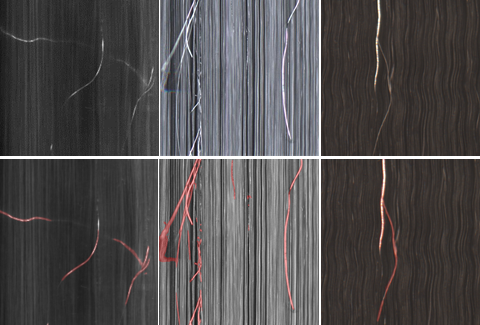
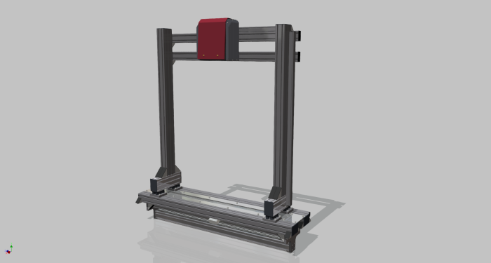
Imaging systems are being developed for detecting transverse filaments and fibre bundles (lint) during carbon fibre manufacturing (Image: Fraunhofer IGCV)
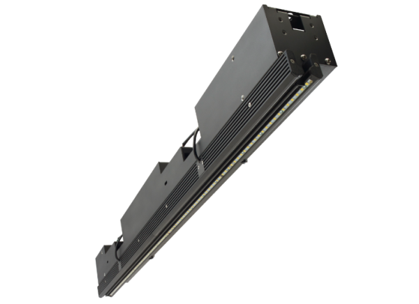
The new system relies on Chromasens’ allPIXA wave line scan camera and Corona II LED line scan light to achieve seamless and continuous surface monitoring. The Corona II is capable of delivering up to 3,500,000 lux, which is essential for producing high-contrast images of deep-black materials such as carbon fibre. The Air Carbon III can detect protruding filaments, lint, and similar foreign bodies, and distinguish each type of defect.
The significantly higher resolution of the CMOS colour line sensor, rather than conventional CCD sensors, is what makes the detection of protruding filaments possible, which range from 7-12µm in diameter. Since the sensors are limited in their measurement width, a novel optical concept was designed and implemented that triples the camera's field of view while keeping the data volume the same. The system was designed primarily for large-format line sensors (up to 85mm), but it is easily transferable to smaller sensors or area sensors. This makes the solution particularly suitable for scaling, as additional hardware costs on the camera side and for computing capacity can be avoided.
Overall, the partners succeeded in developing an inline monitoring system with which carbon fibre production can be continuously and automatically monitored. As of August 2022, the partners were in the final phase of development, carrying out tests in the pilot plant of SGL Carbon and evaluating the data.
Ultra-thin glass manufacturing on the rise
In the glass industry, the demand for glass wafer material – the production of which can be monitored using web inspection solutions – is rising rapidly across a range of industries.
Glass wafers are very thin sections of glass material. They can be made from a range of materials including quartz, borosilicate glass, or fused silica, and are used in a wide variety of applications, such as 3D imaging and sensing; wafer-level packaging; micro-electromechanical systems (MEMS); microfluidics; automotive displays and electronics; microdisplays; and the fabrication of integrated circuits.
“Glass producers are developing the high-scale industrialisation of new ultra-thin glasses for foldable applications or wafer applications,” says Bertrand Mercier, Vice President of Isra Vision’s Glass Business Unit. “Roll-to-roll glass processes are becoming more and more a reality and could open up new markets. Complex shapes are also increasingly required, such as for automotive displays.”
Imaging solutions are increasingly being used to inspect thin glass materials for defects, which are used in the manufacture of automotive and smartphone displays (Image: Isra Vision)
Taking this last example, attractive automotive glass can only be achieved when there are no optical distortions in the glass wafer. A glass inspection system, such as those offered by Isra Vision, must therefore distinguish between flawless and waste products in order to guarantee the highest level of quality.
“Beside the detection of typical ‘visible defects’, functional defects such as surface contamination or microscopic defects are gaining in importance,” says Mercier. “In addition, measurement of physical properties such as curvature, thickness and stress are becoming standard in modern factories.”
The use of glass wafers with new and advanced optical properties is also increasing in the production of TVs and smartphones. Here the wafers offer high transparency, high heat resistance and low thermal expansion. For smartphones in particular, glass wafers are often used to protect the sensors, electronics and semiconductors present in the device.
Isra Vision’s Flat Panel Master is an example of the firm’s systems seeing successful adoption in the inline inspection of thin glass substrates. The system can detect and classify even the tiniest of defects on the surface or edge of glass substrates, while also monitoring particle contamination. At the same time, it collects and analyses inspection data to provide insights into defect causes, allowing users to improve their production processes. In addition to thin glass, the Flat Panel Master can also be used for inspecting float glass, pattern glass, automotive glass and solar glass.
Lead image: Shutterstock/Alexey Ryazanov