Charge-coupled devices (CCDs) have been established in the market as solid-state image sensors for nearly 40 years. They consist of a matrix of light sensitive elements (pixels) fabricated from silicon, with the term CCD referring to the way the signal (the photo generated charges) is moved around the sensor, either from pixel to pixel, or from pixel to a readout register, depending on the different design of CCD available.
The term CMOS (complementary metal oxide semi-conductor) image sensor, on the other hand, does not refer to how the device operates or acquires an image – it simply refers to the fact that the image sensor has been made utilising a CMOS semi-conductor fabrication process, basically the same as that used to make memory chips or other types of electrical integrated circuits.
Gareth Powell, of e2v, says: ‘The development of CMOS sensors has been extremely rapid, when compared with that of CCDs, as the former has come from a standing start just 10 years or so ago to a place where it competes head on with a technology that has been around for 40 years.’
Most commercially-available CMOS image sensors consist of a matrix of individual silicon photodiode pixels as the light sensing elements. The charge generated in each individual element is stored within the capacitance of the detector pixel, and then is read out via a digital shift register that is fabricated from the same piece of silicon as the photodiode pixels.
In addition, the CMOS sensor would then usually contain a charge amplifier circuit to amplify the small electrical signals generated from each pixel. This may take the form of a single amplifier in the readout register of the CMOS device (similar to CCD construction) or there may be an individual amplifier fabricated for each individual photodetector pixel, in which case the device is usually referred to as an active-pixel sensor (APS).
Performance
In general terms, CCD sensors offer better signal-to-noise ratio than CMOS since the analogue charges can be moved around the CCD without inducing any noise – although, currently, according to Tim Stokes, general sales manager at Hamamatsu, there are not huge differences in terms of pixel count, image quality or fundamental sensitivity between CCDs and some CMOS image sensors.
e2v’s Powell adds: ‘Many of the early problems associated with CMOS, such as issues with noise management, have now been largely ironed out – and, indeed, in some cases like high-speed imaging, the signal-to-noise ratio is better than that achieved via CCD.’
The choice between CCD and CMOS sensors depends largely on the application. ‘Many assume that CMOS is best suited to low-end applications, but, for example, very fast line scan applications have to be CMOS,’ explains Joachim Linkemann of Basler. ‘This is because CCD sensors get too hot at these fast speeds, and this affects the image quality.’
Indeed, the smearing or blooming associated with CCD makes CMOS more suitable for other applications, such as onboard cameras to aid reversing vehicles, or lane management systems. ‘CMOS is also particularly suited to outdoor applications, as it can cope with a high dynamic range (more than 120dB),’ says Linkemann. However, he states that CCD remains the best performer in low-light conditions, where it can be up to 10 times better.
‘The majority of applications can now be satisfied with CMOS sensors, except perhaps those at the very high end, for example in astronomy,’ comments Tim Baeyens, founder and business development director at CMOSIS. Previously, CMOS struggled with sensitivity and dark current (unwanted current generated by pixels in the absence of light), but recent advances in pinned photodiode pixel technology have helped to solve this. Baeyens notes that other advances include the use of backside thinning, which enables complete pixels to be made more sensitive. This is particularly useful in UV applications, such as metrology, where even a marginal gain in sensitivity is worthwhile.
‘CMOS has many advantages over CCD, largely due to the fact that much of the supporting microelectronics, such as analogue-to-digital converters – and in some cases even the image processing – is carried out on the CMOS chip itself,’ says Baeyens.
Mark Butler, product manager at Dalsa notes that the on-chip A/D converters allow data to be sent much faster than with CCD sensors. ‘A CMOS sensor can reach data transfer speeds of hundreds of Megapixels per second as opposed to 60 Megapixels per second for CCD,’ he says. It’s difficult to quickly drive analogue signals off-chip with CCDs hence the slower rate.

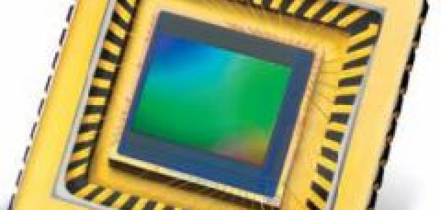
CMOS sensors manufactured by Hamamatsu.
In addition, Powell of e2v comments: ‘With the A/D conversion and image processing occurring on-chip (where for CCD this happens off-chip), there are reductions in cost at system level, which also includes significantly reduced power management requirements too.’ This leads to a reduction in the size and weight of the chip.
Cost
Many imaging applications are cost sensitive and although CMOS sensors are generally thought of as being cheaper than CCD, prices vary depending on the volumes produced. Stokes, of Hamamatsu, comments: ‘A lot is said about CMOS devices being cheaper than CCD technology; in mass consumer markets where millions of chips are made every week then this is certainly true, but in the mid-range scientific and industrial markets where tens of thousands of devices may be manufactured each week, there is not a hugely significant cost difference in terms of the fabrication costs of the silicon.’
Linkemann, of Basler, explains further: ‘Many of the best-performing CMOS sensors are used in the consumer market, but that is because there is volume there. Adding integrated circuits to CMOS sensors improves performance, but at a cost, and unless you can order millions of units, it is not a cost that is worth it – and, as there is not yet great volume in the machine vision market, such highperforming CMOS sensors are not seen so much in our industry.’
Future
CMOS development continues at a pace, and there are many improvements just around the corner. Dalsa’s Butler says: ‘There are a lot of engineering tricks that can be added to the design of CMOS sensors to improve sensitivity and reduce noise. Fixed pattern noise is now close to the levels found in CCD sensors and, in four years’ time, the gap will be much smaller, if there is any at all. However, for applications where image quality is paramount and the summing of charge on chip is beneficial, such as in astronomy sectors, CCDs will always be more suitable.
‘As the process design steps improve to provide smaller features and fit more technology on the chip CMOS will benefit in ever-further improvements in image quality. CMOS technology is still relatively new in the machine vision industry and it’s at a much younger developmental stage than CCD. The technology and process design steps are different in producing a CMOS sensor and therefore the potential artefacts visible in the image are different. CMOS will close the gap with CCD in terms of image quality, but it will require time.’
Basler’s Linkemann adds: ‘In the future, CMOS will work on the areas in which it is deficient, such as low light sensitivity and colour sensitivity, but CCD is a long way from being dead. CCD developers have much more experience, and it is a very stable technology that has a lot of life left in it yet.’
Hamamatsu’s Stokes also believes the future is bright for CMOS: ‘What we can say is that there are many new higher speed CMOS devices now entering the market for high speed industrial imaging applications, these applications previously exclusively used CCDs. Hamamatsu have a number of high speed linear CMOS sensors under development, which will be released to the market sometime in 2009. These are in many ways replacements for previous CCD devices used for industrial imaging applications.’
E2v’s Powell concludes: ‘It’s difficult to say just how much further the development of CMOS sensors will go. Just five or so years ago, the optical limit of a pixel was deemed to be around 3μm. Now, developers are talking about sub-micron levels through back-illumination techniques. What is interesting, though, is how this BSI technology is being deemed as a revelation in CMOS imaging, but in reality has been implemented on high-end CCDs for as long as 20 years. I believe that further innovation in CMOS will come from adopting sophisticated methods that have been applied to CCD to get the highest achievable performance.
‘CMOS technology will continue to develop further, but CCD is not standing still either. There is a likely split between application areas where the scientific, aerospace and specialist applications will remain CCD for a long time to come, and industrial applications will be mixed, with CMOS growing faster. They will continue to battle out the resolution race together.’
Additional reporting by Greg Blackman