We know that CMOS technology has been replacing CCD in most applications during the past 20 years, but Rafael Romay-Juarez, the Executive VP and General Manager at Teledyne Imaging Machine Vision Sensors, believes this is just the start of a more transformational opportunity.
CMOS technology has enabled reducing the complexity of cameras by bringing to the sensor:
- Timing generation
- Power biasing
- ADC and control
More and more functionality has been incorporated to CMOS sensors, up to the point that the pixel array is now not the dominant fraction of the die size.
Rafael-Juarez told the audience at the EMVA Business Conference in Seville, Spain, that 3D stacked sensors are an opportunity to bring more and more functionality into CMOS image sensors in a cost-effective manner.
“We are now at a point where processes that were very difficult 20 years ago are now becoming a reality,” he says.
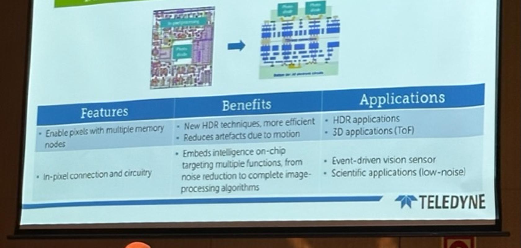
In explaining what opportunities, performances and functionalities are enabled by 3D stacking, he says it increases the fill factor (responsivity) for those pixels with in-pixel extra circuitry. There are feature improvements in that pixels can have multiple memory nodes and in-pixel connection and circuitry. Benefits are that new HDR techniques are more efficient, with a reduction in artefacts due to motion. There is an opportunity to embed intelligence on-chip, targeting multiple functions from noise reduction to complete image-processing algorithms.
The technology removes periphery circuits, reducing the die size, which reduces the total size of the system, offering cost savings in high volumes. There are additional advantages in butted sensors and the prospect of hexagonal and octagonal devices, enabling curved sensing surfaces. This could be used in high-volume applications, endoscopy, camera miniaturisation, X-ray applications and, of course, AR and VR.
Increased parallelism includes features such as multi-tap and multi-sampling readout, with benefits such as a mitigation of bottlenecks introduced by column-parallel ADCs, noise reduction, yield improvement and increased resilience. There is a range of likely applications for space sensors and environments where lower noise volume is critical.
3D stacking integrates new functions, leading to application-specific smart sensors, offering features such as spare areas to include Ips and plug-and-play Ips. The benefits include application-specific embedded functions, greater differentiation and, in general terms, reduces requirements at a system level. Other benefits include SERDES, an MIPI interface and on-chip micro controllers and processors.
Mixing processes and technologies have features such as logic in advance technology node, logic wafers dedicated to memories, logic wafers for communications and there are three stacked layers under development. Benefits will include high-speed SERDES and improvements in image processing, optical and Rx communications and higher integration capabilities.
Benefits from back-side illumination technology include a lower RC time-constant, an increased number of output lines, a better fill factor, enhancements in UV sensitivity and scattering structures and DTI. This will increase the speed of control and readout lines and output bandwidth and sensitivity. This will reduce the amount of required emitted light (if it’s an active illumination) and improvements in NIR and lower-cross talk.
For BSI-stacked, wafers will consist of two layers – a sensor wafer and a logic wafer. A sensor wafer will contain many pixels, via areas to interconnect with the logic wafer and aluminium pads for bonding wires. Process options are Epi Thickness maximising QE in the wavelengths of interest; Deep Trenches Isolation (DTI) full/partial or dual DTI; TSV and/or Cu to Cu-hybrid.
A logic wafer consists of up to eight metals, a SRAM layer, and DMOS or MIM for capacitors, and contains all mixed-signal elements to operate the pixel, digitise and output data. The wafer has readout, pixel array selection and interface circuitry, serialises the data and delivers it to IO ports, offers IO ESD protection at this level and has 65nm and 40nm options
“Is this expensive – or does it sound expensive?” asked Rafael-Juarez of the audience at the business conference today, before revealing there’s an opportunity to buy a much more powerful product at approximately the same price. Teledyne’s 3DS sensor in TPSCo at 65nm is estimated to offer a production cost saving of 30% when compared to a sensor with on-chip processing for industrial application.